M28R400CT, M28R400CB
BUS OPERATIONS
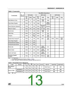
There are six standard bus operations that control
the device. These are Bus Read, Bus Write, Out-
put Disable, Standby, Automatic Standby and Re-
set. See Table 2., Bus Operations, for a summary.
See Figures 9 and 10, Write AC Waveforms, and
Tables 16 and 17, Write AC Characteristics, for
details of the timing requirements.
Output Disable. The data outputs are high im-
Typically glitches of less than 5ns on Chip Enable
or Write Enable are ignored by the memory and do
not affect bus operations.
pedance when the Output Enable is at VIH.
Standby. Standby disables most of the internal
circuitry allowing a substantial reduction of the cur-
rent consumption. The memory is in stand-by
when Chip Enable is at VIH and the device is in
read mode. The power consumption is reduced to
the stand-by level and the outputs are set to high
impedance, independently from the Output Enable
or Write Enable inputs. If Chip Enable switches to
VIH during a program or erase operation, the de-
vice enters Standby mode when finished.
Automatic Standby. Automatic Standby pro-
vides a low power consumption state during Read
mode. Following a read operation, the device en-
ters Automatic Standby after 150ns of bus inactiv-
ity even if Chip Enable is Low, VIL, and the supply
current is reduced to IDD1. The data Inputs/Out-
puts will still output data if a bus Read operation is
in progress.
Reset. During Reset mode when Output Enable
is Low, VIL, the memory is deselected and the out-
puts are high impedance. The memory is in Reset
mode when Reset is at VIL. The power consump-
tion is reduced to the Standby level, independently
from the Chip Enable, Output Enable or Write En-
able inputs. If Reset is pulled to VSS during a Pro-
gram or Erase, this operation is aborted and the
memory content is no longer valid.
Read. Read Bus operations are used to output
the contents of the Memory Array, the Electronic
Signature, the Status Register and the Common
Flash Interface. Both Chip Enable and Output En-
able must be at VIL in order to perform a read op-
eration. The Chip Enable input should be used to
enable the device. Output Enable should be used
to gate data onto the output. The data read de-
pends on the previous command written to the
memory (see COMMAND INTERFACE section).
See Figure 8., Read AC Waveforms, , and Table
15., Read AC Characteristics, for details of when
the output becomes valid.
Read mode is the default state of the device when
exiting Reset or after power-up.
Write. Bus Write operations write Commands to
the memory or latch Input Data to be programmed.
A write operation is initiated when Chip Enable
and Write Enable are at VIL with Output Enable at
VIH. Commands, Input Data and Addresses are
latched on the rising edge of Write Enable or Chip
Enable, whichever occurs first.
Table 2. Bus Operations
V
Operation
Bus Read
E
G
W
RP
WP
X
DQ0-DQ15
Data Output
Data Input
Hi-Z
PP
V
V
V
IH
V
Don't Care
V or V
DD
IL
IL
IL
IL
IH
IH
IH
V
V
V
V
V
V
V
V
Bus Write
Output Disable
Standby
X
IL
IH
PPH
V
X
Don't Care
Don't Care
Don't Care
IH
IH
V
X
X
X
Hi-Z
IH
IH
V
IL
Reset
X
X
X
X
Hi-Z
Note: X = V or V , V = 12V ± 5%.
PPH
IL
IH
9/48

 NUMONYX [ NUMONYX B.V ]