M28R400CT, M28R400CB
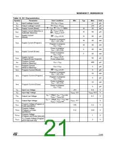
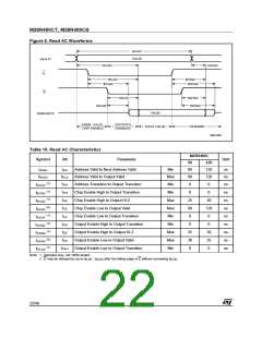
Figure 8. Read AC Waveforms
tAVAV
VALID
A0-A17
E
tAVQV
tAXQX
tELQV
tELQX
tEHQX
tEHQZ
G
tGLQV
tGHQX
tGHQZ
tGLQX
VALID
DQ0-DQ15
ADDR. VALID
CHIP ENABLE
OUTPUTS
ENABLED
DATA VALID
STANDBY
AI04144b
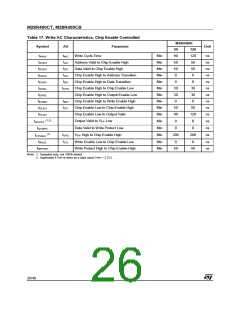
Table 15. Read AC Characteristics
M28R400C
Symbol
Alt
Parameter
Unit
90
120
120
120
t
t
Address Valid to Next Address Valid
Address Valid to Output Valid
Min
Max
Min
90
90
0
ns
ns
ns
AVAV
RC
t
t
ACC
AVQV
(1)
t
Address Transition to Output Transition
0
0
t
OH
AXQX
EHQX
EHQZ
(1)
(1)
(2)
(1)
(1)
(1)
(2)
(1)
t
Chip Enable High to Output Transition
Chip Enable High to Output Hi-Z
Min
Max
Max
Min
0
25
90
0
ns
ns
ns
ns
ns
ns
ns
ns
t
t
OH
t
HZ
30
120
0
t
Chip Enable Low to Output Valid
t
t
CE
ELQV
ELQX
t
LZ
Chip Enable Low to Output Transition
Output Enable High to Output Transition
Output Enable High to Output Hi-Z
Output Enable Low to Output Valid
Output Enable Low to Output Transition
t
Min
0
0
t
t
OH
GHQX
t
DF
Max
Max
Min
25
30
0
30
35
0
GHQZ
t
t
t
OE
GLQV
GLQX
t
OLZ
Note: 1. Sampled only, not 100% tested.
2. G may be delayed by up to t
- t
after the falling edge of E without increasing t
.
ELQV GLQV
ELQV
22/48

 NUMONYX [ NUMONYX B.V ]