M28R400CT, M28R400CB
SIGNAL DESCRIPTIONS
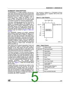
See Figure 2., Logic Diagram and Table 1., Signal
Names, for a brief overview of the signals connect-
ed to this device.
Address Inputs (A0-A17). The Address Inputs
select the cells in the memory array to access dur-
ing Bus Read operations. During Bus Write opera-
tions they control the commands sent to the
Command Interface of the internal state machine.
Data Input/Output (DQ0-DQ15). The Data I/O
outputs the data stored at the selected address
during a Bus Read operation or inputs a command
or the data to be programmed during a Write Bus
operation.
Chip Enable (E). The Chip Enable input acti-
vates the memory control logic, input buffers, de-
coders and sense amplifiers. When Chip Enable is
at VILand Reset is at VIH the device is in active
mode. When Chip Enable is at VIH the memory is
deselected, the outputs are high impedance and
the power consumption is reduced to the stand-by
level.
Output Enable (G). The Output Enable controls
data outputs during the Bus Read operation of the
memory.
Write Enable (W). The Write Enable controls the
Bus Write operation of the memory’s Command
Interface. The data and address inputs are latched
on the rising edge of Chip Enable, E, or Write En-
able, W, whichever occurs first.
state. When Reset is at VIH, the device is in normal
operation. Exiting reset mode the device enters
read array mode, but a negative transition of Chip
Enable or a change of the address is required to
ensure valid data outputs.
V
DD Supply Voltage (1.65V to 2.2V). VDD
provides the power supply to the internal core of
the memory device. It is the main power supply for
all operations (Read, Program and Erase).
VDDQ Supply Voltage (1.65V to 2.2V). VDDQ
provides the power supply to the I/O pins and en-
ables all Outputs to be powered independently
from VDD. VDDQ can be tied to VDD or can use a
separate supply.
VPP Program Supply Voltage. VPP is both a
control input and a power supply pin. The two
functions are selected by the voltage range ap-
plied to the pin. The Supply Voltage VDD and the
Program Supply Voltage VPP can be applied in
any order.
If VPP is kept in a low voltage range (0V to 3.6V)
VPP is seen as a control input. In this case a volt-
age lower than VPPLK gives protection against pro-
gram or block erase, while VPP > VPP1 enables
these functions (see Table 14., DC Characteris-
tics, for the relevant values). VPP is only sampled
at the beginning of a program or block erase; a
change in its value after the operation has started
does not have any effect and program or erase op-
erations continue.
Write Protect (WP). Write Protect is an input
that gives an additional hardware protection for
each block. When Write Protect is at VIL, the Lock-
Down is enabled and the protection status of the
block cannot be changed. When Write Protect is at
VIH, the Lock-Down is disabled and the block can
be locked or unlocked. (refer to Table 6., Read
Protection Register and Lock Register).
Reset (RP). The Reset input provides a hard-
ware reset of the memory. When Reset is at VIL,
the memory is in reset mode: the outputs are high
impedance and the current consumption is mini-
mized. After Reset all blocks are in the Locked
If VPP is in the range 11.4V to 12.6V it acts as a
power supply pin. In this condition VPP must be
stable until the Program/Erase algorithm is com-
pleted (see Table 16 and 17).
VSS Ground. VSS is the reference for all voltage
measurements.
Note: Each device in a system should have
VDD, VDDQ and VPP decoupled with a 0.1µF ca-
pacitor close to the pin. See Figure 7., AC Mea-
surement Load Circuit. The PCB track widths
should be sufficient to carry the required VPP
program and erase currents.
8/48

 NUMONYX [ NUMONYX B.V ]