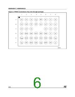
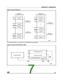
M28R400CT, M28R400CB
COMMAND INTERFACE
All Bus Write operations to the memory are inter-
preted by the Command Interface. Commands
consist of one or more sequential Bus Write oper-
ations. An internal Program/Erase Controller han-
dles all timings and verifies the correct execution
of the Program and Erase commands. The Pro-
gram/Erase Controller provides a Status Register
whose output may be read at any time during, to
monitor the progress of the operation, or the Pro-
gram/Erase states. See APPENDIX D., Table 30.,
Write State Machine Current/Next, sheet 1 of 2.,
for a summary of the Command Interface.
The Command Interface is reset to Read mode
when power is first applied, when exiting from Re-
set or whenever VDD is lower than VLKO. Com-
mand sequences must be followed exactly. Any
invalid combination of commands will reset the de-
vice to Read mode. Refer to Table 3., Commands,
in conjunction with the text descriptions below.
cations to automatically match their interface to
the characteristics of the device. One Bus Write
cycle is required to issue the Read Query Com-
mand. Once the command is issued subsequent
Bus Read operations read from the Common
Flash Interface Memory Area. See APPENDIX B.,
COMMON FLASH INTERFACE (CFI), Tables 24,
25, 26, 27, 28 and 29 for details on the information
contained in the Common Flash Interface memory
area.
Block Erase Command
The Block Erase command can be used to erase
a block. It sets all the bits within the selected block
to ’1’. All previous data in the block is lost. If the
block is protected then the Erase operation will
abort, the data in the block will not be changed and
the Status Register will output the error.
Two Bus Write cycles are required to issue the
command.
Read Memory Array Command
■
The first bus cycle sets up the Erase
command.
The Read command returns the memory to its
Read mode. One Bus Write cycle is required to is-
sue the Read Memory Array command and return
the memory to Read mode. Subsequent read op-
erations will read the addressed location and out-
put the data. When a device Reset occurs, the
memory defaults to Read mode.
■
The second latches the block address in the
internal state machine and starts the Program/
Erase Controller.
If the second bus cycle is not Write Erase Confirm
(D0h), Status Register bits b4 and b5 are set and
the command aborts.
Erase aborts if Reset turns to VIL. As data integrity
cannot be guaranteed when the Erase operation is
aborted, the block must be erased again.
During Erase operations the memory will accept
the Read Status Register command and the Pro-
gram/Erase Suspend command, all other com-
mands will be ignored. Typical Erase times are
given in Table 7., Program, Erase Times and Pro-
gram/Erase Endurance Cycles.
See APPENDIX C., Figure 18., Block Erase Flow-
chart and Pseudo Code, for a suggested flowchart
for using the Block Erase command.
Read Status Register Command
The Status Register indicates when a program or
erase operation is complete and the success or
failure of the operation itself. Issue a Read Status
Register command to read the Status Register’s
contents. Subsequent Bus Read operations read
the Status Register at any address, until another
command is issued. See Table 10., Status Regis-
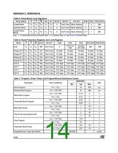
ter Bits, for details on the definitions of the bits.
The Read Status Register command may be is-
sued at any time, even during a Program/Erase
operation. Any Read attempt during a Program/
Erase operation will automatically output the con-
tent of the Status Register.
Chip Erase Command
Read Electronic Signature Command
The Chip Erase command can be used to erase
the entire chip. It sets all of the bits in unprotected
blocks of the memory to ’1’. All previous data is
lost. Two Bus Write operations are required to is-
sue the Chip Erase Command.
The Read Electronic Signature command reads
the Manufacturer and Device Codes and the Block
Locking Status, or the Protection Register.
The Read Electronic Signature command consists
of one write cycle, a subsequent read will output
the Manufacturer Code, the Device Code, the
Block Lock and Lock-Down Status, or the Protec-
tion and Lock Register. See Tables 4, 5 and 6 for
the valid address.
■
The first bus cycle sets up the Chip Erase
command.
■
The second confirms the Chip Erase
command and starts the Program/Erase
Controller.
Read CFI Query Command
The command can be issued to any address. If
any blocks are protected then these are ignored
and all the other blocks are erased. If all of the
blocks are protected the Chip Erase operation ap-
The Read Query Command is used to read data
from the Common Flash Interface (CFI) Memory
Area, allowing programming equipment or appli-
10/48

 NUMONYX [ NUMONYX B.V ]