M25PX64
List of figures
List of figures
Figure 1.
Figure 2.
Figure 3.
Figure 4.
Figure 5.
Figure 6.
Figure 7.
Figure 8.
Figure 9.
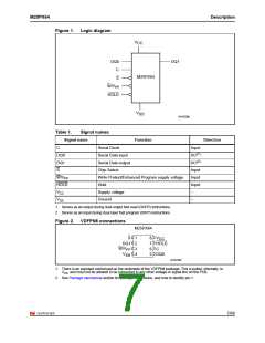
Logic diagram . . . . . . . . . . . . . . . . . . . . . . . . . . . . . . . . . . . . . . . . . . . . . . . . . . . . . . . . . . . . 7
VDFPN8 connections . . . . . . . . . . . . . . . . . . . . . . . . . . . . . . . . . . . . . . . . . . . . . . . . . . . . . . 7
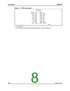
SO16 connections . . . . . . . . . . . . . . . . . . . . . . . . . . . . . . . . . . . . . . . . . . . . . . . . . . . . . . . . 8
Bus master and memory devices on the SPI bus. . . . . . . . . . . . . . . . . . . . . . . . . . . . . . . . 11
SPI modes supported . . . . . . . . . . . . . . . . . . . . . . . . . . . . . . . . . . . . . . . . . . . . . . . . . . . . . 12
Hold condition activation. . . . . . . . . . . . . . . . . . . . . . . . . . . . . . . . . . . . . . . . . . . . . . . . . . . 18
Block diagram . . . . . . . . . . . . . . . . . . . . . . . . . . . . . . . . . . . . . . . . . . . . . . . . . . . . . . . . . . . 19
Write enable (WREN) instruction sequence . . . . . . . . . . . . . . . . . . . . . . . . . . . . . . . . . . . . 28
Write disable (WRDI) instruction sequence . . . . . . . . . . . . . . . . . . . . . . . . . . . . . . . . . . . . 29
Figure 10. Read identification (RDID) instruction sequence and data-out sequence . . . . . . . . . . . . . 31
Figure 11. Read status register (RDSR) instruction sequence and data-out sequence . . . . . . . . . . . 33
Figure 12. Write status register (WRSR) instruction sequence . . . . . . . . . . . . . . . . . . . . . . . . . . . . . . 34
Figure 13. Read data bytes (READ) instruction sequence and data-out sequence . . . . . . . . . . . . . . 36
Figure 14. Read data bytes at higher speed (FAST_READ) instruction sequence
and data-out sequence. . . . . . . . . . . . . . . . . . . . . . . . . . . . . . . . . . . . . . . . . . . . . . . . . . . . 37
Figure 15. Dual output fast read instruction sequence . . . . . . . . . . . . . . . . . . . . . . . . . . . . . . . . . . . . 38
Figure 16. Read lock register (RDLR) instruction sequence and data-out sequence . . . . . . . . . . . . . 39
Figure 17. Read OTP (ROTP) instruction and data-out sequence . . . . . . . . . . . . . . . . . . . . . . . . . . . 40
Figure 18. Page program (PP) instruction sequence. . . . . . . . . . . . . . . . . . . . . . . . . . . . . . . . . . . . . . 42
Figure 19. Dual input fast program (DIFP) instruction sequence. . . . . . . . . . . . . . . . . . . . . . . . . . . . . 44
Figure 20. Program OTP (POTP) instruction sequence . . . . . . . . . . . . . . . . . . . . . . . . . . . . . . . . . . . 46
Figure 21. How to permanently lock the 64 OTP bytes . . . . . . . . . . . . . . . . . . . . . . . . . . . . . . . . . . . . 46
Figure 22. Write to lock register (WRLR) instruction sequence . . . . . . . . . . . . . . . . . . . . . . . . . . . . . . 47
Figure 23. Subsector erase (SSE) instruction sequence . . . . . . . . . . . . . . . . . . . . . . . . . . . . . . . . . . . 48
Figure 24. Sector erase (SE) instruction sequence . . . . . . . . . . . . . . . . . . . . . . . . . . . . . . . . . . . . . . . 49
Figure 25. Bulk erase (BE) instruction sequence. . . . . . . . . . . . . . . . . . . . . . . . . . . . . . . . . . . . . . . . . 50
Figure 26. Deep power-down (DP) instruction sequence . . . . . . . . . . . . . . . . . . . . . . . . . . . . . . . . . . 51
Figure 27. Release from deep power-down (RDP) instruction sequence . . . . . . . . . . . . . . . . . . . . . . 52
Figure 28. Power-up timing . . . . . . . . . . . . . . . . . . . . . . . . . . . . . . . . . . . . . . . . . . . . . . . . . . . . . . . . . 54
Figure 29. AC measurement I/O waveform . . . . . . . . . . . . . . . . . . . . . . . . . . . . . . . . . . . . . . . . . . . . . 56
Figure 30. Serial input timing . . . . . . . . . . . . . . . . . . . . . . . . . . . . . . . . . . . . . . . . . . . . . . . . . . . . . . . . 59
Figure 31. Write protect setup and hold timing during WRSR when SRWD=1 . . . . . . . . . . . . . . . . . . 60
Figure 32. Hold timing . . . . . . . . . . . . . . . . . . . . . . . . . . . . . . . . . . . . . . . . . . . . . . . . . . . . . . . . . . . . . 60
Figure 33. Output timing . . . . . . . . . . . . . . . . . . . . . . . . . . . . . . . . . . . . . . . . . . . . . . . . . . . . . . . . . . . 61
Figure 34. VPPH timing. . . . . . . . . . . . . . . . . . . . . . . . . . . . . . . . . . . . . . . . . . . . . . . . . . . . . . . . . . . . . 61
Figure 35. VDFPN8 (MLP8) 8-lead very thin dual flat package no lead,
8 × 6 mm, package outline . . . . . . . . . . . . . . . . . . . . . . . . . . . . . . . . . . . . . . . . . . . . . . . . . 62
Figure 36. SO16 wide - 16-lead plastic small outline, 300 mils body width, package outline . . . . . . . 63
Figure 37. TBGA, 6x8 mm, 24 ball package outline . . . . . . . . . . . . . . . . . . . . . . . . . . . . . . . . . . . . . . 64
5/68

 NUMONYX [ NUMONYX B.V ]