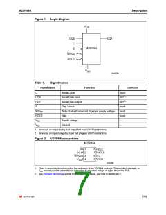
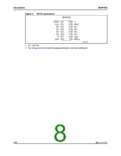
M25PX64
SPI modes
3
SPI modes
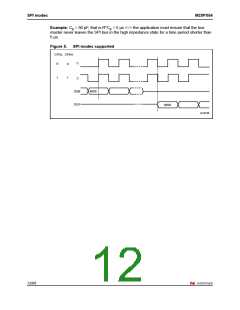
These devices can be driven by a microcontroller with its SPI peripheral running in either of
the two following modes:
CPOL=0, CPHA=0
CPOL=1, CPHA=1
For these two modes, input data is latched in on the rising edge of Serial Clock (C), and
output data is available from the falling edge of Serial Clock (C).
The difference between the two modes, as shown in Figure 5, is the clock polarity when the
bus master is in standby mode and not transferring data:
C remains at 0 for (CPOL=0, CPHA=0)
C remains at 1 for (CPOL=1, CPHA=1)
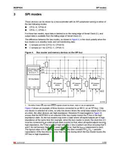
Figure 4. Bus master and memory devices on the SPI bus
VSS
VCC
R
SDO
SPI interface with
(CPOL, CPHA) =
(0, 0) or (1, 1)
SDI
SCK
C
VCC
VCC
VCC
C
C
VSS
VSS
VSS
SPI Bus Master
DQ1DQ0
DQ1 DQ0
DQ1DQ0
SPI memory
device
SPI memory
device
SPI memory
device
R
R
R
CS3 CS2 CS1
W
S
S
S
W
HOLD
HOLD
HOLD
W
AI13725b
1. The Write Protect (W) and Hold (HOLD) signals should be driven, High or Low as appropriate.
Figure 4 shows an example of three devices connected to an MCU, on an SPI bus. Only
one device is selected at a time, so only one device drives the serial data output (DQ1) line
at a time, the other devices are high impedance. Resistors R (represented in Figure 4)
ensure that the M25PX64 is not selected if the bus master leaves the S line in the high
impedance state. As the bus master may enter a state where all inputs/outputs are in high
impedance at the same time (for example, when the bus master is reset), the clock line (C)
must be connected to an external pull-down resistor so that, when all inputs/outputs become
high impedance, the S line is pulled High while the C line is pulled Low (thus ensuring that S
and C do not become High at the same time, and so, that the tSHCH requirement is met).
The typical value of R is 100 kΩ, assuming that the time constant R*Cp (Cp = parasitic
capacitance of the bus line) is shorter than the time during which the bus master leaves the
SPI bus in high impedance.
11/68

 NUMONYX [ NUMONYX B.V ]