M25P32
Description
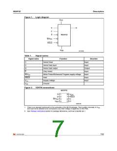
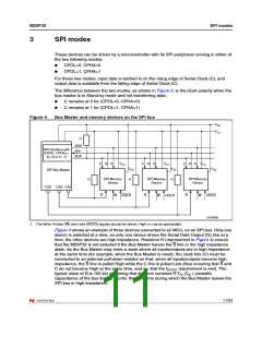
Figure 1.
Logic diagram
V
CC
D
C
S
Q
M25P32
W/V
PP
HOLD
V
SS
AI07483b
Table 1.
Signal names
Signal name
Function
Direction
C
Serial Clock
Input
Input
Output
Input
Input
Input
Input
D
Serial Data input
Serial Data output
Chip Select
Q
S
W/VPP
HOLD
VCC
VSS
Write Protect/Enhanced Program supply voltage
Hold
Supply voltage
Ground
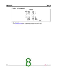
Figure 2.
VDFPN connections
M25P32
S
Q
1
8
7
6
5
V
CC
HOLD
2
3
4
W/V
C
D
PP
SS
V
AI08518b
1. There is an exposed central pad on the underside of the MLP8 package. This is pulled, internally, to VSS
,
and must not be allowed to be connected to any other voltage or signal line on the PCB.
2. See Package mechanical section for package dimensions, and how to identify pin-1.
7/53

 NUMONYX [ NUMONYX B.V ]