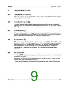
M25P32
List of figures
List of figures
Figure 1.
Figure 2.
Figure 3.
Figure 4.
Figure 5.
Figure 6.
Figure 7.
Figure 8.
Figure 9.
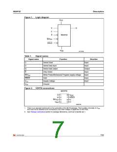
Logic diagram . . . . . . . . . . . . . . . . . . . . . . . . . . . . . . . . . . . . . . . . . . . . . . . . . . . . . . . . . . . . 7
VDFPN connections . . . . . . . . . . . . . . . . . . . . . . . . . . . . . . . . . . . . . . . . . . . . . . . . . . . . . . . 7
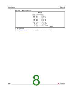
SO connections . . . . . . . . . . . . . . . . . . . . . . . . . . . . . . . . . . . . . . . . . . . . . . . . . . . . . . . . . . 8
Bus Master and memory devices on the SPI bus. . . . . . . . . . . . . . . . . . . . . . . . . . . . . . . . 11
SPI modes supported . . . . . . . . . . . . . . . . . . . . . . . . . . . . . . . . . . . . . . . . . . . . . . . . . . . . . 12
Hold condition activation. . . . . . . . . . . . . . . . . . . . . . . . . . . . . . . . . . . . . . . . . . . . . . . . . . . 16
Block diagram. . . . . . . . . . . . . . . . . . . . . . . . . . . . . . . . . . . . . . . . . . . . . . . . . . . . . . . . . . . 17
Write Enable (WREN) instruction sequence. . . . . . . . . . . . . . . . . . . . . . . . . . . . . . . . . . . . 21
Write Disable (WRDI) instruction sequence . . . . . . . . . . . . . . . . . . . . . . . . . . . . . . . . . . . . 22
Figure 10. Read Identification (RDID) instruction sequence and data-out sequence . . . . . . . . . . . . . 23
Figure 11. Read Status Register (RDSR) instruction sequence and data-out sequence . . . . . . . . . . 25
Figure 12. Write Status Register (WRSR) instruction sequence . . . . . . . . . . . . . . . . . . . . . . . . . . . . . 26
Figure 13. Read Data Bytes (READ) instruction sequence and data-out sequence . . . . . . . . . . . . . . 28
Figure 14. Read Data Bytes at Higher Speed (FAST_READ) instruction sequence
and data-out sequence . . . . . . . . . . . . . . . . . . . . . . . . . . . . . . . . . . . . . . . . . . . . . . . . . . . . 29
Figure 15. Page Program (PP) instruction sequence . . . . . . . . . . . . . . . . . . . . . . . . . . . . . . . . . . . . . 31
Figure 16. Sector Erase (SE) instruction sequence. . . . . . . . . . . . . . . . . . . . . . . . . . . . . . . . . . . . . . . 32
Figure 17. Bulk Erase (BE) instruction sequence . . . . . . . . . . . . . . . . . . . . . . . . . . . . . . . . . . . . . . . . 33
Figure 18. Deep Power-down (DP) instruction sequence . . . . . . . . . . . . . . . . . . . . . . . . . . . . . . . . . . 34
Figure 19. Release from Deep Power-down and Read Electronic Signature (RES)
instruction sequence and data-out sequence. . . . . . . . . . . . . . . . . . . . . . . . . . . . . . . . . . . 36
Figure 20. Release from Deep Power-down (RES) instruction sequence . . . . . . . . . . . . . . . . . . . . . . 36
Figure 21. Power-up timing . . . . . . . . . . . . . . . . . . . . . . . . . . . . . . . . . . . . . . . . . . . . . . . . . . . . . . . . . 38
Figure 22. AC measurement I/O waveform . . . . . . . . . . . . . . . . . . . . . . . . . . . . . . . . . . . . . . . . . . . . . 40
Figure 23. Serial input timing . . . . . . . . . . . . . . . . . . . . . . . . . . . . . . . . . . . . . . . . . . . . . . . . . . . . . . . . 43
Figure 24. Write Protect Setup and Hold timing during WRSR when SRWD=1 . . . . . . . . . . . . . . . . . 44
Figure 25. Hold timing . . . . . . . . . . . . . . . . . . . . . . . . . . . . . . . . . . . . . . . . . . . . . . . . . . . . . . . . . . . . . 44
Figure 26. Output timing . . . . . . . . . . . . . . . . . . . . . . . . . . . . . . . . . . . . . . . . . . . . . . . . . . . . . . . . . . . 45
Figure 27.
V
timing. . . . . . . . . . . . . . . . . . . . . . . . . . . . . . . . . . . . . . . . . . . . . . . . . . . . . . . . . . . . . 45
PPH
Figure 28. VDFPN8 (MLP8) 8-lead Very thin Dual Flat Package No lead, 8 × 6 mm,
package outline. . . . . . . . . . . . . . . . . . . . . . . . . . . . . . . . . . . . . . . . . . . . . . . . . . . . . . . . . . 46
Figure 29. SO16 wide – 16-lead Plastic Small Outline, 300 mils body width, package outline . . . . . . 47
Figure 30. VFQFPN8 (MLP8) 8-lead Very thin Fine Pitch Quad Flat Package No lead,
6 × 5 mm, package outline . . . . . . . . . . . . . . . . . . . . . . . . . . . . . . . . . . . . . . . . . . . . . . . . . 48
Figure 31. SO8W 8 lead Plastic Small Outline, 208 mils body width, package outline . . . . . . . . . . . . 49
5/53

 NUMONYX [ NUMONYX B.V ]