M25P32
Revision history
13
Revision history
Table 20. Document revision history
Date
Revision
Changes
28-Apr-2003
15-May-2003
20-Jun-2003
18-Jul-2003
0.1
0.2
0.3
0.4
Target Specification Document written in brief form
Target Specification Document written in full
8x6 MLP8 and SO16(300 mil) packages added
tPP, tSE and tBE revised
SO16 package code changed. Output Timing Reference Voltage
changed.
24-Sep-2003
0.5
Table of contents, warning about exposed paddle on MLP8, and Pb-free
options added.
04-Dec-2003
0.6
Value of tVSL(min) VWI, tPP(typ) and tBE(typ) changed. Change of naming
for VDFPN8 package.
10-Dec-2003
01-Apr-2004
05-Aug-2004
01-Oct-2004
1.0
2.0
3.0
4.0
Document promoted to Product Preview
Document promoted to Preliminary Data. Soldering temperature
information clarified for RoHS compliant devices. Device grade
information clarified
Device grade information further clarified
Document promoted to mature datasheet. Footnotes removed from P and
G options in Ordering Information table. Minor wording improvements
made.
Read Identification (RDID), Deep Power-down (DP) and Release from
Deep Power-down and Read Electronic Signature (RES) instructions, and
Active Power, Standby Power and Deep Power-down modes paragraph
clarified.
01-Apr-2005
01-Aug-2005
5.0
6.0
Updated Page Program (PP) instructions in Page Programming, Page
Program (PP) and Table 14: AC characteristics.
Fast Program/Erase mode added and Power-up specified for Fast
Program/Erase mode in Power-up and Power-down section. W pin
changed to W/VPP. (see Write Protect/Enhanced Program supply voltage
(W/VPP) description).
23-Jan-2006
7.0
tVPPHSL added to Table 14: AC characteristics and tPP for Fast
Program/Erase mode added. Figure 27: VPPH timing inserted. Note 2
added below Figure 28 All packages are ECOPACK® compliant. Blank
option removed under Plating Technology in Table 19
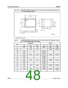
VDFPN8 package specifications updated (see Section 11: Package
mechanical).
10-Feb-2006
28-Nov-2006
8.0
9
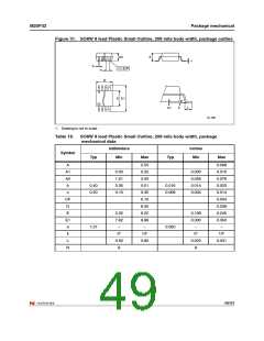
MLP8 5 × 6 mm and SO8W packages added (see Section 11: Package
mechanical). VCC supply voltage and VSS ground descriptions added.
Figure 4: Bus Master and memory devices on the SPI bus updated and
explanation added below.
Table 9: Absolute maximum ratings: VIO max modified and TLEAD added.
Products in T9HX technology introduced (see Table 14: AC
characteristics (T9HX technology)). Small text changes.
51/53

 NUMONYX [ NUMONYX B.V ]