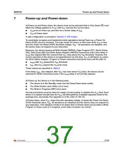
Power-up and Power-down
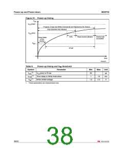
Figure 21. Power-up timing
M25P32
V
CC
V
(max)
CC
Program, Erase and Write Commands are Rejected by the Device
Chip Selection Not Allowed
V
(min)
CC
tVSL
Read Access allowed
Device fully
accessible
Reset State
of the
Device
V
WI
tPUW
time
AI04009C
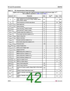
Table 8.
Power-up timing and V threshold
WI
Symbol
Parameter
Min.
Max.
Unit
(1)
tVSL
VCC(min) to S low
30
1
µs
ms
V
(1)
tPUW
Time delay to Write instruction
Write Inhibit voltage
10
(1)
VWI
1.5
2.5
1. These parameters are characterized only.
38/53

 NUMONYX [ NUMONYX B.V ]