M25P32
Instructions
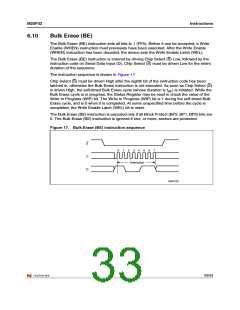
6.7
Read Data Bytes at Higher Speed (FAST_READ)
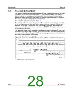
The device is first selected by driving Chip Select (S) Low. The instruction code for the Read
Data Bytes at Higher Speed (FAST_READ) instruction is followed by a 3-byte address (A23-
A0) and a dummy byte, each bit being latched-in during the rising edge of Serial Clock (C).
Then the memory contents, at that address, is shifted out on Serial Data Output (Q), each
bit being shifted out, at a maximum frequency f , during the falling edge of Serial Clock (C).
C
The instruction sequence is shown in Figure 14.
The first byte addressed can be at any location. The address is automatically incremented
to the next higher address after each byte of data is shifted out. The whole memory can,
therefore, be read with a single Read Data Bytes at Higher Speed (FAST_READ)
instruction. When the highest address is reached, the address counter rolls over to
000000h, allowing the read sequence to be continued indefinitely.
The Read Data Bytes at Higher Speed (FAST_READ) instruction is terminated by driving
Chip Select (S) High. Chip Select (S) can be driven High at any time during data output. Any
Read Data Bytes at Higher Speed (FAST_READ) instruction, while an Erase, Program or
Write cycle is in progress, is rejected without having any effects on the cycle that is in
progress.
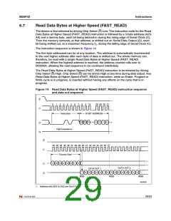
Figure 14. Read Data Bytes at Higher Speed (FAST_READ) instruction sequence
and data-out sequence
S
0
1
2
3
4
5
6
7
8
9
10
28 29 30 31
C
Instruction
24 BIT ADDRESS
23 22 21
3
2
1
0
D
Q
High Impedance
S
C
47
32 33 34 35 36 37 38 39 40 41 42 43 44 45 46
Dummy Byte
7
6
5
4
3
2
0
1
D
Q
DATA OUT 2
DATA OUT 1
7
6
5
4
3
2
1
0
7
7
6
5
4
3
2
0
1
MSB
MSB
MSB
AI04006
1. Address bits A23 to A22 are Don’t Care.
29/53

 NUMONYX [ NUMONYX B.V ]