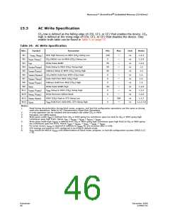
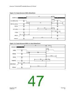
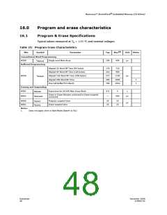
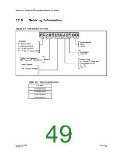
®
Numonyx™ StrataFlash Embedded Memory (J3-65nm)
Appendix A Reference Information
A.1
Common Flash Interface
The CFI specification outlines device and host system software interrogation handshake
which allows specific vendor-specified software algorithms to be used for entire families
of devices. This allows device independent, JEDEC ID-independent, and forward- and
backward-compatible software support for the specified flash device families. It allows
flash vendors to standardize their existing interfaces for long-term compatibility.
This section defines the data structure or “database” returned by the CFI Query
command. System software should parse this structure to gain critical information such
as block size, density, x8/x16, and electrical specifications. Once this information has
been obtained, the software will know which command sets to use to enable flash
writes, block erases, and otherwise control the flash component. The Query is part of
an overall specification for multiple command set and control interface descriptions
called CFI.
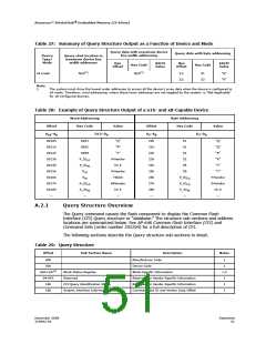
A.2
Query Structure Output
The Query “database” allows system software to gain information for controlling the
flash component. This section describes the device’s CFI-compliant interface that allows
the host system to access Query data.
Query data are always presented on the lowest-order data outputs (D[7:0]) only. The
numerical offset value is the address relative to the maximum bus width supported by
the device. On this family of devices, the Query table device starting address is a 10h,
which is a word address for x16 devices.
For a word-wide (x16) device, the first two bytes of the Query structure, “Q” and “R” in
ASCII, appear on the low byte at word addresses 10h and 11h. This CFI-compliant
device outputs 00h data on upper bytes. Thus, the device outputs ASCII “Q” in the low
byte (D[7:0]) and 00h in the high byte (D[15:8]).
At Query addresses containing two or more bytes of information, the least significant
data byte is presented at the lower address, and the most significant data byte is
presented at the higher address.
In all of the following tables, addresses and data are represented in hexadecimal
notation, so the “h” suffix has been dropped. In addition, since the upper byte of word-
wide devices is always “00h,” the leading “00” has been dropped from the table
notation and only the lower byte value is shown. Any x16 device outputs can be
assumed to have 00h on the upper byte in this mode.
Table 27: Summary of Query Structure Output as a Function of Device and Mode
Query data with maximum device
Query data with byte addressing
bus width addressing
Device
Type/
Mode
Query start location in
maximum device bus
width addresses
Hex
Offset
ASCII
Value
Hex
Offset
ASCII
Value
Hex Code
Hex Code
x16 device
x16 mode
10h
10:
11:
12:
0051
0052
0059
“Q”
“R”
“Y”
20:
21:
22:
51
00
52
“Q”
“Null”
“R”
x16 device
20:
51
“Q”
Datasheet
50
December 2008
319942-02

 NUMONYX [ NUMONYX B.V ]