PDF
最近搜索
热门搜索
发布采购

| 型号: | 160FT |
| PDF下载: | 下载PDF文件 查看货源 |
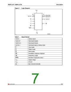
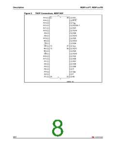
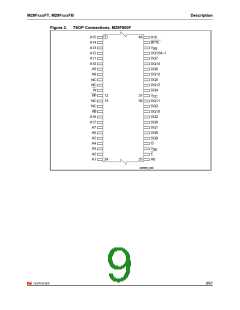
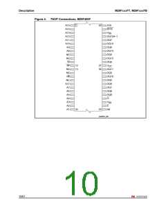
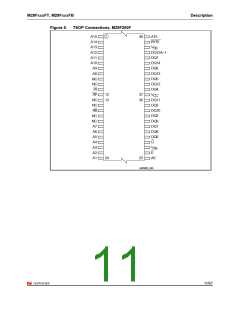
| 内容描述: | 顶部/底部引导块5 V电源快闪记忆体 [Top / Bottom Boot Block 5 V Supply Flash Memory] |
| 分类和应用: | |
| 文件页数/大小: | 67 页 / 1730 K |
| 品牌: |  NUMONYX [ NUMONYX B.V ] NUMONYX [ NUMONYX B.V ] |
专业IC领域供求交易平台:提供全面的IC Datasheet资料和资讯,Datasheet 1000万数据,IC品牌1000多家。