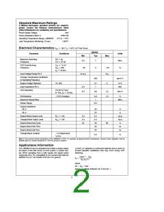
Absolute Maximum Ratings
If Military/Aerospace specified devices are required,
please contact the National Semiconductor Sales
Office/Distributors for availability and specifications.
Power Supply Voltage
26V
Power Dissipation (Note 1)
1000 mW
a
0 C to 70 C
Operating Temperature Range, LM566CN
Lead Temperature (Soldering, 10 sec.)
§
§
a
260 C
§
e
e
12V, T
A
Electrical Characteristics V
25 C, AC Test Circuit
§
CC
LM566C
Typ
Parameter
Conditions
Units
Min
Max
e
e
Maximum Operating
Frequency
R0
C0
2k
0.5
1
0
MHz
2.7 pF
e
e
VCO Free-Running
Frequency
C
R
1.5 nF
20k
O
b
a
30
30
%
O
e
f
O
10 kHz
Input Voltage Range Pin 5
*/4 V
CC
V
CC
Average Temperature Coefficient
of Operating Frequency
200
ppm/ C
§
Supply Voltage Rejection
Input Impedance Pin 5
VCO Sensitivity
10–20V
0.1
1
2
%/V
0.5
6.0
MX
For Pin 5, From
e
6.6
7.2
1.5
kHz/V
8–10V, f
10 kHz
O
g
FM Distortion
10% Deviation
0.2
1
%
Maximum Sweep Rate
Sweep Range
MHz
10:1
Output Impedance
Pin 3
50
50
5.4
2.4
50
20
50
X
X
Pin 4
e
e
Square Wave Output Level
Triangle Wave Output Level
Square Wave Duty Cycle
Square Wave Rise Time
Square Wave Fall Time
Triangle Wave Linearity
R
R
10k
10k
5.0
2.0
40
Vp-p
Vp-p
%
L1
L2
60
ns
ns
a
(/2 V
1V Segment at
0.5
%
CC
Note 1: The maximum junction temperature of the LM566CN is 150 C. For operation at elevated junction temperatures, maximum power dissipation must be
§
derated based on a thermal resistance of 115 C/W, junction to ambient.
§
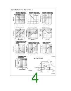
Applications Information
The LM566CN may be operated from either a single supply
A 0.001 mF capacitor is connected between pins 5 and 6 to
prevent parasitic oscillations that may occur during VCO
switching.
g
as shown in this test circuit, or from a split ( ) power sup-
ply. When operating from a split supply, the square wave
output (pin 3) is TTL compatible (2 mA current sink) with the
addition of a 4.7 kX resistor from pin 3 to ground.
2.4(Va
V )
5
b
e
f
O
R
O
C
O
Va
where
k
k
20K
2K
R
O
and V is voltage between pin 5 and pin 1.
5
2

 NSC [ National Semiconductor ]