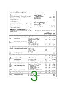
Absolute Maximum Ratings (Notes 6,
5)
ESD Susceptibility (Note 8)
Junction Temperature (Note 9)
Soldering Information
T Package (10 seconds)
Storage Temperature
Thermal Resistance
θJC
3000V
150˚C
If Military/Aerospace specified devices are required,
please contact the National Semiconductor Sales Office/
Distributors for availability and specifications.
260˚C
−40˚C to +150˚C
Supply Voltage |V+|+|V−|
1˚C/W
(No Signal)
94V
84V
Supply Voltage |V+|+|V−|
(Input Signal)
θJA
43˚C/W
(V+ or V−) and
Operating Ratings (Notes 5, 6)
Common Mode Input Voltage
|V+| + |V−| ≤ 80V
Temperature Range
Differential Input Voltage (Note 16)
Output Current
60V
Internally Limited
125W
TMIN ≤ TA ≤ TMAX
Supply Voltage |V+| + |V−|
−20˚C ≤ TA ≤ +85˚C
20V to 84V
Power Dissipation (Note 7)
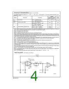
Electrical Characteristics (Notes 5, 6)
−
The following specifications apply for V+ +28V, V
−28V, IMUTE −0.5 mA with RL 4Ω unless otherwise specified. Limits
=
=
=
=
=
apply for TA 25˚C.
LM3886
Units
Symbol
Parameter
Conditions
Typical
Limit
(Limits)
(Note 10) (Note 11)
|V+| + |V−| Power Supply Voltage (Note 14)
Vpin7 − V− ≥ 9V
20
V (min)
V (max)
18
84
AM
Mute Attenuation
Pin 8 Open or at 0V, Mute: On
>
Current out of Pin 8 0.5 mA,
115
80
dB (min)
Mute: Off
=
THD + N 0.1% (max)
PO
Output Power (Continuous Average)
= =
1 kHz; f 20 kHz
(Note 4)
f
+
−
=
=
=
=
=
=
=
|V | |V | 28V, RL 4Ω
68
38
50
60
30
W (min)
W (min)
W
+
−
|V | |V | 28V, RL 8Ω
+
−
=
=
|V | |V | 35V, RL 8Ω
Peak PO
THD + N
Instantaneous Peak Output Power
Total Harmonic Distortion Plus Noise
135
W
=
60W, RL 4Ω,
%
%
=
30W, RL 8Ω,
0.03
0.03
20 Hz ≤ f ≤ 20 kHz
=
AV 26 dB
=
=
SR
(Note 4)
Slew Rate (Note 13)
VIN 2.0Vp-p, tRISE 2 ns
V/µs
(min)
19
50
1
8
I+ (Note 4) Total Quiescent Power Supply
VCM 0V, Vo 0V, Io 0A
=
=
=
85
10
mA (max)
mV (max)
Current
= =
VCM 0V, Io 0 mA
VOS
(Note 3)
Input Offset Voltage
=
=
IB
Input Bias Current
VCM 0V, Io 0 mA
0.2
1
0.2
7
µA (max)
µA (max)
A (min)
=
=
IOS
Io
Input Offset Current
VCM 0V, Io 0 mA
0.01
11.5
+
−
= = = =
|V | |V | 20V, tON 10 ms, VO 0V
Output Current Limit
=
=
Vod
(Note 3)
Output Dropout Voltage (Note 15)
|V+–VO|, V+ 28V, Io +100 mA
1.6
2.5
2.0
3.0
V (max)
V (max)
|VO–V−|, V− −28V, Io −100 mA
−
=
=
=
=
−40V,
PSRR
Power Supply Rejection Ratio
V+ 40V to 20V, V
120
85
dB (min)
= =
VCM 0V, Io 0 mA
(Note 3)
−
V+ 40V, V
105
85
dB (min)
=
=
−40V to −20V,
=
=
VCM 0V, Io 0 mA
−
=
=
−20V to −60V,
= =
VCM 20V to −20V, Io 0 mA
CMRR
(Note 3)
Common Mode Rejection Ratio
Open Loop Voltage Gain
Gain-Bandwidth Product
V+ 60V to 20V, V
110
115
8
85
90
2
dB (min)
dB (min)
+
−
= = = =
|V | |V | 28V, RL 2 kΩ, ∆VO 40V
AVOL
(Note 3)
+
−
=
=
GBWP
|V | |V | 30V
MHz
(min)
=
=
fO 100 kHz, VIN 50 mVrms
3
www.national.com

 NSC [ National Semiconductor ]