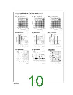
ous loads in the Typical Performance Characteristics sec-
tion, giving an accurate figure for the maximum thermal
resistance required for a particular amplifier design. This
Application Information (Continued)
Over-Voltage Protection: The LM3886 contains overvolt-
age protection circuitry that limits the output current to ap-
proximately 11Apeak while also providing voltage clamping,
though not through internal clamping diodes. The clamping
effect is quite the same, however, the output transistors are
designed to work alternately by sinking large current spikes.
=
=
data was based on θJC 1˚C/W and θCS 0.2˚C/W. We also
provide a section regarding heat sink determination for any
audio amplifier design where θCS may be a different value. It
should be noted that the idea behind dissipating the maxi-
mum power within the IC is to provide the device with a low
resistance to convection heat transfer such as a heat sink.
Therefore, it is necessary for the system designer to be con-
servative in his heat sink calculations. As a rule, the lower
the thermal resistance of the heat sink the higher the amount
of power that may be dissipated. This is of course guided by
the cost and size requirements of the system. Convection
cooling heat sinks are available commercially, and their
manufacturers should be consulted for ratings.
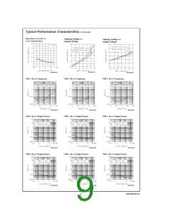
SPiKe Protection: The LM3886 is protected from instanta-
neous peak-temperature stressing by the power transistor
array. The Safe Operating Area graph in the Typical Perfor-
mance Characteristics section shows the area of device
operation where the SPiKe Protection Circuitry is not en-
abled. The waveform to the right of the SOA graph exempli-
fies how the dynamic protection will cause waveform distor-
tion when enabled.
Proper mounting of the IC is required to minimize the thermal
drop between the package and the heat sink. The heat sink
must also have enough metal under the package to conduct
heat from the center of the package bottom to the fins with-
out excessive temperature drop.
Thermal Protection: The LM3886 has a sophisticated ther-
mal protection scheme to prevent long-term thermal stress
to the device. When the temperature on the die reaches
165˚C, the LM3886 shuts down. It starts operating again
when the die temperature drops to about 155˚C, but if the
temperature again begins to rise, shutdown will occur again
at 165˚C. Therefore the device is allowed to heat up to a
relatively high temperature if the fault condition is temporary,
but a sustained fault will cause the device to cycle in a
Schmitt Trigger fashion between the thermal shutdown tem-
perature limits of 165˚C and 155˚C. This greatly reduces the
stress imposed on the IC by thermal cycling, which in turn
improves its reliability under sustained fault conditions.
A thermal grease such as Wakefield type 120 or Thermalloy
Thermacote should be used when mounting the package to
the heat sink. Without this compound, thermal resistance will
be no better than 0.5˚C/W, and probably much worse. With
the compound, thermal resistance will be 0.2˚C/W or less,
assuming under 0.005 inch combined flatness runout for the
package and heat sink. Proper torquing of the mounting
bolts is important and can be determined from heat sink
manufacturer’s specification sheets.
Since the die temperature is directly dependent upon the
heat sink, the heat sink should be chosen as discussed in
the Thermal Considerations section, such that thermal
shutdown will not be reached during normal operation. Using
the best heat sink possible within the cost and space con-
straints of the system will improve the long-term reliability of
any power semiconductor device.
Should it be necessary to isolate V−
from the heat sink, an in-
sulating washer is required. Hard washers like beryluum ox-
ide, anodized aluminum and mica require the use of thermal
compound on both faces. Two-mil mica washers are most
common, giving about 0.4˚C/W interface resistance with the
compound.
Silicone-rubber washers are also available. A 0.5˚C/W ther-
mal resistance is claimed without thermal compound. Expe-
rience has shown that these rubber washers deteriorate and
must be replaced should the IC be dismounted.
THERMAL CONSIDERATIONS
Heat Sinking
The choice of a heat sink for a high-power audio amplifier is
made entirely to keep the die temperature at a level such
that the thermal protection circuitry does not operate under
normal circumstances. The heat sink should be chosen to
dissipate the maximum IC power for a given supply voltage
and rated load.
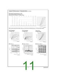
Determining Maximum Power Dissipation
Power dissipation within the integrated circuit package is a
very important parameter requiring a thorough understand-
ing if optimum power output is to be obtained. An incorrect
maximum power dissipation (PD) calculation may result in in-
adequate heat sinking, causing thermal shutdown circuitry to
operate and limit the output power.
With high-power pulses of longer duration than 100 ms, the
case temperature will heat up drastically without the use of a
heat sink. Therefore the case temperature, as measured at
the center of the package bottom, is entirely dependent on
heat sink design and the mounting of the IC to the heat sink.
For the design of a heat sink for your audio amplifier applica-
tion refer to the Determining The Correct Heat Sink sec-
tion.
The following equations can be used to acccurately calculate
the maximum and average integrated circuit power dissipa-
tion for your amplifier design, given the supply voltage, rated
load, and output power. These equations can be directly ap-
plied to the Power Dissipation vs Output Power curves in the
Typical Performance Characteristics section.
Since a semiconductor manufacturer has no control over
which heat sink is used in a particular amplifier design, we
can only inform the system designer of the parameters and
the method needed in the determination of a heat sink. With
this in mind, the system designer must choose his supply
voltages, a rated load, a desired output power level, and
know the ambient temperature surrounding the device.
These parameters are in addition to knowing the maximum
junction temperature and the thermal resistance of the IC,
both of which are provided by National Semiconductor.
Equation (1) exemplifies the maximum power dissipation of
the IC and Equations (2), (3) exemplify the average IC power
dissipation expressed in different forms.
PDMAX VCC2/2π2RL
(1)
=
where VCC is the total supply voltage
=
PDAVE (VOpk/RL)[VCC/π − VOpk/2]
(2)
=
where VCC is the total supply voltage and VOpk VCC/π
As a benefit to the system designer we have provided Maxi-
mum Power Dissipation vs Supply Voltages curves for vari-
13
www.national.com

 NSC [ National Semiconductor ]