range applications. If the current limit is set based upon 25˚C
ratings, then false current limiting can occur at high tempera-
ture.
Design Information (Continued)
P-Channel MOSFET Selection (Q1)
The important parameters for the PFET are the maximum
Drain-Source voltage (VDS), the on resistance (RDSON), Cur-
rent rating, and the input capacitance.
Keeping the gate capacitance below 2000pF is recom-
mended to keep switching losses and transition times low.
As gate capacitance increases, operating frequency should
be reduced and as gate capacitance decreases operating
frequency can be increased.
The voltage across the PFET when it is turned off is equal to
the sum of the input voltage and the diode forward voltage.
The VDS must be selected to provide some margin beyond
the input voltage. PGATE swings the PFET’s gate from VIN
to VIN − 5V when the input voltage is greater than 7V. At less
than 7V input, the PGATE voltage swing is smaller. At 4.5V
input the PGATE swings from VIN to VIN − 3.3V. To insure
that the PFET turns on completely, a low threshold PFET
should be used when the input voltage is less than 7V.
RDSON and package size must be used to determine the
appropriate FET for a given current as well as peak current
capability. Switching losses also must be considered.
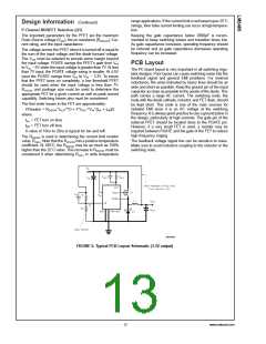
PCB Layout
The PC board layout is very important in all switching regu-
lator designs. Poor layout can cause switching noise into the
feedback signal and general EMI problems. For minimal
inductance, the wires indicated by heavy lines should be as
wide and short as possible. Keep the ground pin of the input
capacitor as close as possible to the anode of the diode. This
path carries a large AC current. The switching node, the
node with the diode cathode, inductor, and FET drain, should
be kept short. This node is one of the main sources for
radiated EMI since it is an AC voltage at the switching
frequency. It is always good practice to use a ground plane in
the design, particularly at high currents. The gate pin of the
external PFET should be located close to the PGATE pin.
However, if a very small FET is used, a resistor may be
required between PGATE and the gate of the FET to reduce
high frequency ringing.
The first order losses in the FET are approximately:
2
*
*
*
*
*
PDswitch = RDSON IOUT D + F IOUT VIN (ton + toff)/2
where:
ton = FET turn on time
toff = FET turn off time
A value of 10ns to 20ns is typical for ton and toff.
The RDSON is used in determining the current limit resistor
value, RADJ. Note that the RDSON has a positive temperature
coefficient. At 100˚C, the RDSON may be as much as 150%
higher than the 25˚C value. This increase in RDSON must be
considered it when determining RADJ in wide temperature
The feedback voltage signal line can be sensitive to noise.
Make sure to avoid inductive coupling to the inductor or the
switching node.
20034628
FIGURE 6. Typical PCB Layout Schematic (3.3V output)
13
www.national.com

 NSC [ National Semiconductor ]