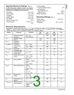
Absolute Maximum Ratings (Note 1)
If Military/Aerospace specified devices are required,
please contact the National Semiconductor Sales Office/
Distributors for availability and specifications.
ESD Susceptibilty
Human Body Model (Note 3)
Lead Temperature
2kV
Vapor Phase (60 sec.)
Infared (15 sec.)
215˚C
220˚C
VIN Voltage
−0.3V to 36V
−0.3V to 36V
−0.3V to 5V
−1.0V to 36V
−0.3V to 36V
150˚C
Storage Temperature
−65˚C to 150˚C
PGATE Voltage
FB Voltage
ISENSE Voltage
ADJ Voltage
Operating Ratings (Note 1)
Supply Voltage
Operating Junction
Temperature
4.5V to 35V
Maximum Junction Temp.
Power Dissipation
@
417mW TA
=
−40˚C to +125˚C
25˚C
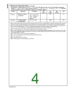
Electrical Characteristics
Specifications in Standard type face are for TJ = 25˚C, and in bold type face apply over the full Operating Temperature
Range (TJ = −40˚C to +125˚C). Unless otherwise specified, VIN = 12V, VISNS = VIN − 1V, and VADJ = VIN − 1.1V. Datasheet
min/max specification limits are guaranteed by design, test, or statistical analysis.
Symbol
Parameter
Conditions
Min
Typ
(Note 5)
250
Max
(Note 4)
400
Unit
(Note 4)
IQ
Quiescent Current at
ground pin
FB = 1.5V
µA
(Not Switching)
VFB
Feedback Voltage
(Note 6)
1.226
1.242
1.258
1.267
15
V
1.217
VHYST
Comparator
10
14
mV
mV
Hysteresis
20
VCL(Note 7)
Current limit
RADJ = 20kΩ
RADJ = 160kΩ
VFB = 1.5V
110
comparator trip
voltage
880
0
VCL_OFFSET
ICL_ADJ
TCL
Current limit
−20
3.0
6
+20
7.0
14
mV
µA
µs
comparator offset
Current limit ADJ
current source
Current limit one shot
off time
VFB = 1.5V
5.5
9
VADJ = 11.5V
VISNS = 11.0V
VFB = 1.0V
Source
RPGATE
Driver resistance
5.5
8.5
Ω
ISOURCE = 100mA
Sink
ISink = 100mA
Source
IPGATE
Driver Output current
0.44
A
VIN = 7V,
PGATE = 3.5V
Sink
0.32
1.2
VIN = 7V,
PGATE = 3.5V
VIN = 4.5V
VFB = 1.0V
IGATE = 100µA sink
VFB = 1.0V
VPGATEMIN
Minimum driver
voltage
V
IFB
FB pin Bias Current
(Note 8)
300
100
750
nA
ns
TONMIN_NOR
Minimum on time in
normal operation
VISNS = VADJ+0.1V
Cload on OUT =
1000pF
(Note 9)
3
www.national.com

 NSC [ National Semiconductor ]