mine if a heatsink is needed, the power dissipated by the
regulator, PD, must be calculated:
Application Hints (Continued)
IIN = IL + IG
PD = (VIN − VOUT) IL + VIN G
I
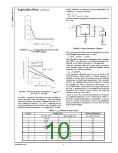
Figure 8 shows the voltage and currents which are present in
the circuit.
00906360
00906357
FIGURE 8. Power Dissipation Diagram
FIGURE 6. θ(J−A) vs Copper (2 ounce) Area for the
SOT-223 Package
The next parameter which must be calculated is the maxi-
mum allowable temperature rise, TR(max):
TR(max) = TJ(max) − TA(max)
where TJ(max) is the maximum allowable junction tempera-
ture (125˚C), and TA(max) is the maximum ambient tem-
perature which will be encountered in the application.
Using the calculated values for TR(max) and PD, the maxi-
mum allowable value for the junction-to-ambient thermal
resistance (θJA) can be calculated:
θJA = TR(max)/PD
If the maximum allowable value for θJA is found to be
≥92˚C/W (Typical Rated Value) for TO-252 package, no
heatsink is needed since the package alone will dissipate
enough heat to satisfy these requirements. If the calculated
value for θJA falls below these limits, a heatsink is required.
As a design aid, Table 1 shows the value of the θJA of
TO-252 for different heatsink area. The copper patterns that
we used to measure these θJAs are shown at the end of the
Application Notes Section. Figure 9 reflects the same test
results as what are in the Table 1
00906358
FIGURE 7. Maximum Power Dissipation vs TAMB for
the SOT-223 Package
Figure 10 shows the maximum allowable power dissipation
vs. ambient temperature for the TO-252 device. Figure 11
shows the maximum allowable power dissipation vs. copper
area (in2) for the TO-252 device. Please see AN1028 for
power enhancement techniques to be used with SOT-223
and TO-252 packages.
The LM317 regulators have internal thermal shutdown to
protect the device from over-heating. Under all possible
operating conditions, the junction temperature of the LM317
must be within the range of 0˚C to 125˚C. A heatsink may be
required depending on the maximum power dissipation and
maximum ambient temperature of the application. To deter-
TABLE 1. θJA Different Heatsink Area
Copper Area
Layout
Thermal Resistance
Top Side (in2)*
Bottom Side (in2)
(θJA˚C/W) TO-252
1
2
3
4
5
6
7
8
9
0.0123
0.066
0.3
0.53
0.76
1
0
0
103
87
60
54
52
47
84
70
63
0
0
0
0
0
0.2
0.4
0.6
0
0
www.national.com
10

 NSC [ National Semiconductor ]