Absolute Maximum Ratings (Note 1)
If Military/Aerospace specified devices are required,
please contact the National Semiconductor Sales Office/
Distributors for availability and specifications.
Storage Temperature
−55˚C to +150˚C
260˚C
Lead Temperature
(Soldering, 4 seconds)
Output is Short Circuit Protected
ESD rating to be determined.
Power Dissipation
Internally Limited
40V
Input-Output Voltage Differential
Operating Junction Temperature
Range
−40˚C to +125˚C
Electrical Characteristics (Note 2)
Parameter
Conditions
Min
Typ
0.01
0.1
Max
0.04
0.5
0.2
100
5
Units
%/V
%
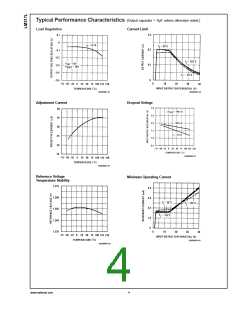
Line Regulation
TJ = 25˚C, 3V ≤ (VIN − VOUT) ≤ 40V, IL ≤ 20mA (Note 3)
TJ = 25˚C, 5mA ≤ IOUT ≤ IMAX, (Note 3)
TJ = 25˚C, 10ms Pulse
Load Regulation
Thermal Regulation
Adjustment Pin Current
Adjustment Pin Current
Change
0.04
50
%/W
µA
5mA ≤ IL ≤ 100mA
0.2
µA
3V ≤ (VIN − VOUT) ≤ 40V, P ≤ 625mW
3V ≤ (VIN − VOUT) ≤ 40V, (Note 4)
5mA ≤ IOUT ≤ 100mA, P ≤ 625mW
3V ≤ (VIN − VOUT) ≤ 40V, IL ≤ 20mA (Note 3)
5mA ≤ IOUT ≤ 100mA, (Note 3)
TMIN ≤ TJ ≤ TMax
Reference Voltage
1.20
1.25
1.30
V
Line Regulation
0.02
0.3
0.07
1.5
%/V
%
Load Regulation
Temperature Stability
Minimum Load Current
0.65
3.5
%
(VIN − VOUT) ≤ 40V
5
mA
3V ≤ (VIN − VOUT) ≤ 15V
3V ≤ (VIN − VOUT) ≤ 13V
(VIN − VOUT) = 40V
1.5
2.5
300
150
Current Limit
100
25
200
50
mA
mA
Rms Output Noise, % of VOUT
Ripple Rejection Ratio
TJ = 25˚C, 10Hz ≤ f ≤ 10kHz
VOUT = 10V, f = 120Hz, CADJ = 0
CADJ = 10µF
0.003
65
%
dB
66
80
dB
Long-Term Stability
Thermal Resistance
Junction to Ambient
TJ = 125˚C, 1000 Hours
Z Package 0.4" Leads
0.3
1
%
180
160
165
290
165
˚C/W
˚C/W
˚C/W
˚C/W
˚C/W
Z Package 0.125 Leads
SO-8 Package
6-Bump micro SMD
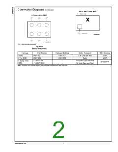
Thermal Rating of SO
Package
Note 1: “Absolute Maximum Ratings” indicate limits beyond which damage to the device may occur. Operating Ratings indicate conditions for which the device is
functional, but do not guarantee specific performance limits.
Note 2: Unless otherwise noted, these specifications apply: −25˚C ≤ T ≤ 125˚C for the LM317L; V − V
= 5V and I
= 40 mA. Although power dissipation
OUT
j
IN
OUT
is internally limited, these specifications are applicable for power dissipations up to 625 mW. I
is 100 mA.
MAX
Note 3: Regulation is measured at constant junction temperature, using pulse testing with a low duty cycle. Changes in output voltage due to heating effects are cov-
ered under the specification for thermal regulation.
Note 4: Thermal resistance of the TO-92 package is 180˚C/W junction to ambient with 0.4" leads from a PC board and 160˚C/W junction to ambient with 0.125" lead
length to PC board.
3
www.national.com

 NSC [ National Semiconductor ]