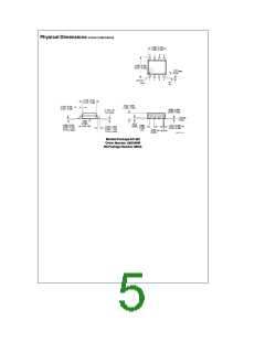
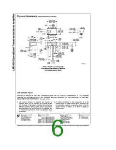
Absolute Maximum Ratings
If Military/Aerospace specified devices are required,
please contact the National Semiconductor Sales
Office/Distributors for availability and specifications.
Amplifier Bias Current (I
DC Input Voltage
)
2 mA
ABC
a
b
V
S
V
S
to
Output Short Circuit Duration
Indefinite
Supply Voltage (Note 2)
LM3080
LM3080A
Operating Temperature Range
LM3080N or LM3080AN
g
g
18V
22V
a
0 C to 70 C
§
65 C to 150 C
§
b
a
Storage Temperature Range
§
§
Power Dissipation
250 mW
Lead Temperature (Soldering, 10 sec.)
260 C
§
g
Differential Input Voltage
5V
Electrical Characteristics (Note 1)
LM3080
Typ
LM3080A
Typ
Parameter
Conditions
Units
Min
Max
Min
Max
Input Offset Voltage
0.4
5
6
0.4
2
5
2
mV
mV
mV
Over Specified Temperature Range
e
I
5 mA
0.3
0.1
0.1
0.3
0.1
0.1
ABC
s
s
Input Offset Voltage Change
Input Offset Current
5 mA
I
500 mA
3
mV
ABC
0.6
0.6
mA
Input Bias Current
0.4
1
5
7
0.4
1
5
8
mA
mA
Over Specified Temperature Range
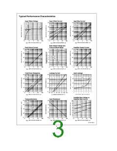
Forward Transconductance (g
Peak Output Current
)
m
6700
9600
13000 7700
4000
9600
12000 mmho
mmho
Over Specified Temperature Range 5400
e
e
e
e
5 mA
R
R
R
0, I
0
5
3
5
7
mA
mA
L
L
L
ABC
350
300
500
650
350
500
650
0
300
mA
Over Specified Temperature Range
Peak Output Voltage
Positive
s
s
s
s
e %
e %
a
b
a
b
a
b
a
b
R
R
, 5 mA
, 5 mA
I
I
500 mA
500 mA
12
12
14.2
14.4
12
12
14.2
14.4
V
V
L
ABC
ABC
Negative
L
Amplifier Supply Current
1.1
1.1
mA
Input Offset Voltage Sensitivity
a
b
Positive
DV
DV
/DV
/DV
20
20
150
150
20
20
150
150
mV/V
mV/V
OFFSET
Negative
OFFSET
Common Mode Rejection Ratio
Common Mode Range
Input Resistance
80
110
80
110
dB
V
g
g
g
g
12
14
12
14
10
26
10
26
kX
e
e
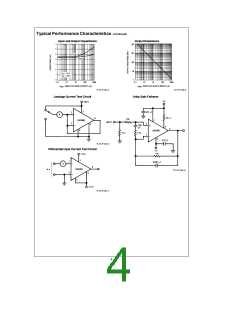
Magnitude of Leakage Current
Differential Input Current
Open Loop Bandwidth
Slew Rate
I
I
0
0.2
0.02
2
100
100
0.2
0.02
2
5
5
nA
ABC
e
g
0, Input
4V
nA
ABC
MHz
V/ms
Unity Gain Compensated
50
50
e
e
e
) 500 mA, unless otherwise specified.
ABC
g
Note 1: These specifications apply for V
15V and T
25 C, amplifier bias current (I
§
Note 2: Selection to supply voltage above 22V, contact the factory.
S
A
g
2

 NSC [ National Semiconductor ]