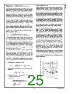
loaded down, may not work correctly. Because of the rela-
tively high startup currents required by the inverting topology,
the Soft-start feature shown in Figure 27 is recommended.
Application Information (Continued)
lNVERTING REGULATOR
The circuit in Figure 27 converts a positive input voltage to a
negative output voltage with a common ground. The circuit
operates by bootstrapping the regulators ground pin to the
negative output voltage, then grounding the feedback pin,
the regulator senses the inverted output voltage and regu-
lates it.
Also shown in Figure 27 are several shutdown methods for
the inverting configuration. With the inverting configuration,
some level shifting is required, because the ground pin of the
regulator is no longer at ground, but is now at the negative
output voltage. The shutdown methods shown accept
ground referenced shutdown signals.
This example uses the LM2598-5 to generate a −5V output,
but other output voltages are possible by selecting other
output voltage versions, including the adjustable version.
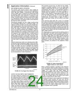
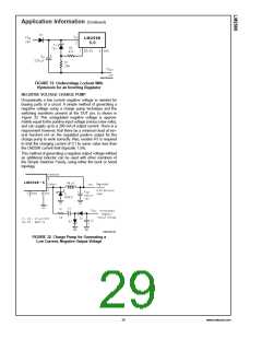
Since this regulator topology can produce an output voltage
that is either greater than or less than the input voltage, the
maximum output current greatly depends on both the input
and output voltage. The curve shown in Figure 28 provides a
guide as to the amount of output load current possible for the
different input and output voltage conditions.
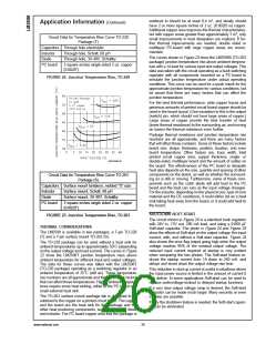
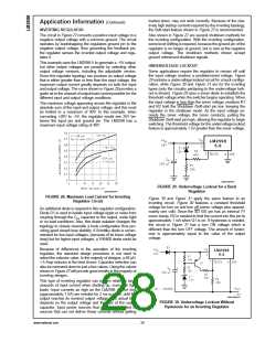
UNDERVOLTAGE LOCKOUT
Some applications require the regulator to remain off until
the input voltage reaches a predetermined voltage. Figure
29 contains a undervoltage lockout circuit for a buck configu-
ration, while Figure 30 and Figure 31 are for the inverting
types (only the circuitry pertaining to the undervoltage lock-
out is shown). Figure 29 uses a zener diode to establish the
threshold voltage when the switcher begins operating. When
the input voltage is less than the zener voltage, resistors R1
and R2 hold the Shutdown /Soft-start pin low, keeping the
regulator in the shutdown mode. As the input voltage ex-
ceeds the zener voltage, the zener conducts, pulling the
Shutdown /Soft-start pin high, allowing the regulator to begin
switching. The threshold voltage for the undervoltage lockout
feature is approximately 1.5V greater than the zener voltage.
The maximum voltage appearing across the regulator is the
absolute sum of the input and output voltage, and this must
be limited to a maximum of 40V. In this example, when
converting +20V to −5V, the regulator would see 25V be-
tween the input pin and ground pin. The LM2598 has a
maximum input voltage rating of 40V.
DS012593-45
FIGURE 29. Undervoltage Lockout for a Buck
Regulator
DS012593-44
FIGURE 28. Maximum Load Current for Inverting
Regulator Circuit
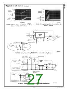
Figure 30 and Figure 31 apply the same feature to an
inverting circuit. Figure 30 features a constant threshold
voltage for turn on and turn off (zener voltage plus approxi-
mately one volt). Since the SD /SS pin has an internal 7V
zener clamp, R2 is needed to limit the current into this pin to
approximately 1 mA when Q1 is on. If hysteresis is needed,
the circuit in Figure 31 has a turn ON voltage which is
different than the turn OFF voltage. The amount of hyster-
esis is approximately equal to the value of the output
voltage.
An additional diode is required in this regulator configuration.
Diode D1 is used to isolate input voltage ripple or noise from
coupling through the CIN capacitor to the output, under light
or no load conditions. Also, this diode isolation changes the
topology to closely resemble a buck configuration thus pro-
viding good closed loop stability. A Schottky diode is recom-
mended for low input voltages, (because of its lower voltage
drop) but for higher input voltages, a 1N5400 diode could be
used.
Because of differences in the operation of the inverting
regulator, the standard design procedure is not used to
select the inductor value. In the majority of designs, a 68 µH,
1.5 Amp inductor is the best choice. Capacitor selection can
also be narrowed down to just a few values. Using the values
shown in Figure 27 will provide good results in the majority of
inverting designs.
This type of inverting regulator can require relatively large
amounts of input current when starting up, even with light
loads. Input currents as high as the LM2598 current limit
(approximately 1.5A) are needed for 2 ms or more, until the
output reaches its nominal output voltage. The actual time
depends on the output voltage and the size of the output
capacitor. Input power sources that are current limited or
sources that can not deliver these currents without getting
DS012593-47
FIGURE 30. Undervoltage Lockout Without
Hysteresis for an Inverting Regulator
www.national.com
28

 NSC [ National Semiconductor ]