with the capacitor placed from the input pin to ground and
the resistor placed between the input supply and the input
pin. Note that the values of RIN and CIN shown in the sche-
matic are good enough for most applications, but some read-
justing might be required for a particular application. If effi-
ciency is a major concern, replace the resistor with a small
inductor (say 10 µH and rated at 100 mA).
Application Hints (Continued)
The duty cycle of a flyback regulator is determined by the fol-
lowing equation:
STABILITY
Theoretically, the maximum output voltage can be as large
as desired — just keep increasing the turns ratio of the trans-
former. However, there exists some physical limitations that
prevent the turns ratio, and thus the output voltage, from in-
creasing to infinity. The physical limitations are capacitances
and inductances in the LM2587 switch, the output diode(s),
and the transformer — such as reverse recovery time of the
output diode (mentioned above).
All current-mode controlled regulators can suffer from an in-
stability, known as subharmonic oscillation, if they operate
with a duty cycle above 50%. To eliminate subharmonic os-
cillations, a minimum value of inductance is required to en-
sure stability for all boost and flyback regulators. The mini-
mum inductance is given by:
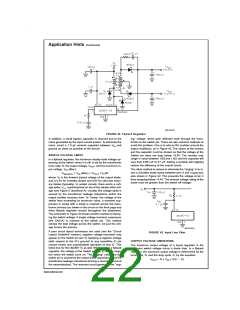
NOISY INPUT LINE CONDITION)
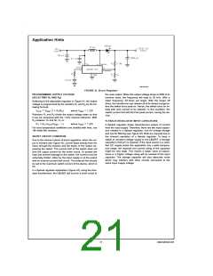
A small, low-pass RC filter should be used at the input pin of
the LM2587 if the input voltage has an unusual large amount
of transient noise, such as with an input switch that bounces.
The circuit in Figure 43 demonstrates the layout of the filter,
where VSAT is the switch saturation voltage and can be
found in the Characteristic Curves.
DS012316-29
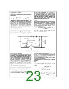
FIGURE 44. Circuit Board Layout
CIRCUIT LAYOUT GUIDELINES
3) Maximum allowed junction temperature (125˚C for the
LM2587). For a safe, conservative design, a temperature ap-
proximately 15˚C cooler than the maximum junction tem-
perature should be selected (110˚C).
As in any switching regulator, layout is very important. Rap-
idly switching currents associated with wiring inductance
generate voltage transients which can cause problems. For
minimal inductance and ground loops, keep the length of the
leads and traces as short as possible. Use single point
grounding or ground plane construction for best results.
Separate the signal grounds from the power grounds (as in-
dicated in Figure 44). When using the Adjustable version,
physically locate the programming resistors as near the
regulator IC as possible, to keep the sensitive feedback wir-
ing short.
4) LM2587 package thermal resistances θJA and θJC (given
in the Electrical Characteristics).
Total power dissipated (PD) by the LM2587 can be estimated
as follows:
Boost:
HEAT SINK/THERMAL CONSIDERATIONS
In many cases, no heat sink is required to keep the LM2587
junction temperature within the allowed operating range. For
each application, to determine whether or not a heat sink will
be required, the following must be identified:
1) Maximum ambient temperature (in the application).
VIN is the minimum input voltage, VOUT is the output voltage,
N is the transformer turns ratio, D is the duty cycle, and ILOAD
2) Maximum regulator power dissipation (in the application).
∑
is the maximum load current (and ILOAD is the sum of the
maximum load currents for multiple-output flyback regula-
tors). The duty cycle is given by:
23
www.national.com

 NSC [ National Semiconductor ]