Application Hints (Continued)
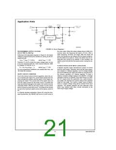
DS012316-27
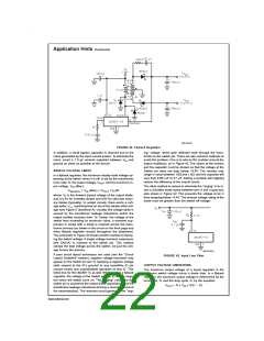
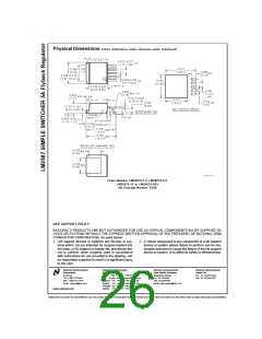
FIGURE 42. Flyback Regulator
In addition, a small bypass capacitor is required due to the
noise generated by the input current pulses. To eliminate the
noise, insert a 1.0 µF ceramic capacitor between VIN and
ground as close as possible to the device.
ing” voltage, which gets reflected back through the trans-
former to the switch pin. There are two common methods to
avoid this problem. One is to add an RC snubber around the
output rectifier(s), as in Figure 42. The values of the resistor
and the capacitor must be chosen so that the voltage at the
Switch pin does not drop below −0.4V. The resistor may
range in value between 10Ω and 1 kΩ, and the capacitor will
vary from 0.001 µF to 0.1 µF. Adding a snubber will (slightly)
reduce the efficiency of the overall circuit.
SWITCH VOLTAGE LIMITS
In a flyback regulator, the maximum steady-state voltage ap-
pearing at the switch, when it is off, is set by the transformer
turns ratio, N, the output voltage, VOUT, and the maximum in-
put voltage, VIN (Max):
The other method to reduce or eliminate the “ringing” is to in-
sert a Schottky diode clamp between pins 4 and 3 (ground),
also shown in Figure 42. This prevents the voltage at pin 4
from dropping below −0.4V. The reverse voltage rating of the
diode must be greater than the switch off voltage.
=
VSW(OFF) VIN (Max) + (VOUT +VF)/N
where VF is the forward biased voltage of the output diode,
and is 0.5V for Schottky diodes and 0.8V for ultra-fast recov-
ery diodes (typically). In certain circuits, there exists a volt-
age spike, VLL, superimposed on top of the steady-state volt-
age (see Figure 5, waveform A). Usually, this voltage spike is
caused by the transformer leakage inductance and/or the
output rectifier recovery time. To “clamp” the voltage at the
switch from exceeding its maximum value, a transient sup-
pressor in series with a diode is inserted across the trans-
former primary (as shown in the circuit on the front page and
other flyback regulator circuits throughout the datasheet).
The schematic in Figure 42 shows another method of clamp-
ing the switch voltage. A single voltage transient suppressor
(the SA51A) is inserted at the switch pin. This method
clamps the total voltage across the switch, not just the volt-
age across the primary.
DS012316-28
If poor circuit layout techniques are used (see the “Circuit
Layout Guideline” section), negative voltage transients may
appear on the Switch pin (pin 4). Applying a negative voltage
(with respect to the IC’s ground) to any monolithic IC pin
causes erratic and unpredictable operation of that IC. This
holds true for the LM2587 IC as well. When used in a flyback
regulator, the voltage at the Switch pin (pin 4) can go nega-
tive when the switch turns on. The “ringing” voltage at the
switch pin is caused by the output diode capacitance and the
transformer leakage inductance forming a resonant circuit at
the secondary(ies). The resonant circuit generates the “ring-
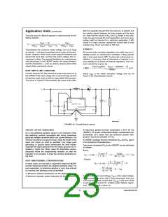
FIGURE 43. Input Line Filter
OUTPUT VOLTAGE LIMITATIONS
The maximum output voltage of a boost regulator is the
maximum switch voltage minus a diode drop. In a flyback
regulator, the maximum output voltage is determined by the
turns ratio, N, and the duty cycle, D, by the equation:
VOUT ≈ N x VIN x D/(1 − D)
www.national.com
22

 NSC [ National Semiconductor ]