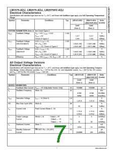
Typical Performance Characteristics (Circuit of Figure 2) (Continued)
Maximum Power Dissipation
Feedback Pin Current
(TO-263) (See (Note 12))
01147528
01147505
Switching Waveforms
Load Transient Response
01147506
01147507
V
= 5V
OUT
A: Output Pin Voltage, 10V/div
B: Output Pin Current, 1A/div
C: Inductor Current, 0.5A/div
D: Output Ripple Voltage, 20 mV/div,
AC-Coupled
Horizontal Time Base: 5 µs/div
Single-point grounding (as indicated) or ground plane con-
struction should be used for best results. When using the
Adjustable version, physically locate the programming resis-
tors near the regulator, to keep the sensitive feedback wiring
short.
Test Circuit and Layout Guidelines
As in any switching regulator, layout is very important. Rap-
idly switching currents associated with wiring inductance
generate voltage transients which can cause problems. For
minimal inductance and ground loops, the length of the leads
indicated by heavy lines should be kept as short as possible.
11
www.national.com

 NSC [ National Semiconductor ]