TL/H/12327–5
CC
TL/H/12327–4
FIGURE 4. Power Dissipation vs V
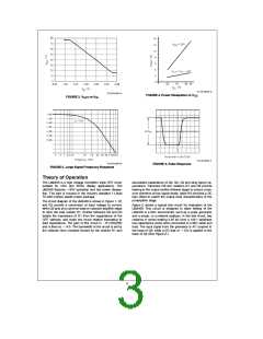
FIGURE 3. V
OUT
vs V
IN
TL/H/12327–7
TL/H/12327–6
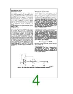
FIGURE 6. Pulse Response
FIGURE 5. Large Signal Frequency Response
Theory of Operation
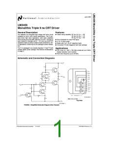
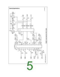
The LM2406 is a high voltage monolithic triple CRT driver
associated capacitance of Q2, Q3, Q4 and stray layout ca-
pacitance. Transistor Q6 and resistors R7 and R8 provide
biasing to the output emitter-follower stage to reduce cross-
over distortion at low signal levels, while R3 provides a DC
bias offset to match the output level characteristics of the
preamplifier stage.
suitable for VGA and SVGA display applications. The
a
LM2406 features 80V operation and low power dissipa-
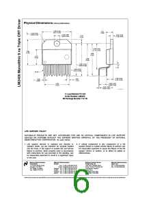
tion. The part is housed in the industry standard 11-lead
TO-220 molded plastic power package.
The circuit diagram of the LM2406 is shown in Figure 1. Q1
and R2 provide a conversion of input voltage to current,
while Q2 acts as a common base or cascode amplifier stage
to drive the load resistor R1. Emitter followers Q3 and Q4
isolate the impedance of R1 from the capacitance of the
CRT cathode, and make the circuit relative insensitive to
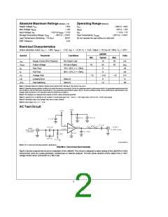
Figure 2 shows a typical test circuit for evaluation of the
LM2406. This circuit is designed to allow testing of the
LM2406 in a 50X environment, such as a pulse generator
and a scope, or a network analyzer. In this test circuit, two
resistors in series totaling 4.95 kX form a 100:1 wideband
low capacitance probe when connected to a 50X cable and
load. The input signal from the generator is AC coupled to
b
load capacitance. The gain of this circuit is R1/(R2 R3)
and is fixed at 14.5. The bandwidth of the circuit is set by
ll
b
a
the base of Q5, while a DC bias of 12V is applied to the
base of Q2 (See Figure 2 ).
the collector time constant formed by the resistor R1 and
3

 NSC [ National Semiconductor ]