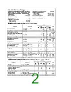
Absolute Maximum Ratings
If Military/Aerospace specified devices are required,
please contact the National Semiconductor Sales
Office/Distributors for availability and specifications.
Output Short Circuit Duration (Note 3)
Continuous
Operating Temperature Range
LH0021/LH0041
LH0021C/LH0041C
b
a
55 C to 125 C
§
§
25 C to 85 C
b a
g
Supply Voltage
18V
§
65 C to 150 C
§
§
b
a
Power Dissipation
See Curves
Storage Temperature Range
§
g
g
Differential Input Voltage
Input Voltage (Note 1)
30V
15V
Lead Temperature (Soldering, 10 sec.)
ESD rating to be determined.
300 C
§
Peak Output Current (Note 2)
LH0021/LH0021C
LH0041/LH0041C
2.0 Amps
0.5 Amps
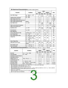
DC Electrical Characteristics for LH0021/LH0021C (Note 4)
Limits
Parameter
Conditions
LH0021
LH0021C
Units
Min Typ Max Min Typ Max
k
k
e
Input Offset Voltage
R
S
R
S
100X, T
100X
25 C
§
1.0 3.0
5.0
3.0 6.0
7.5
mV
mV
C
k
Voltage Drift with Temperature
Offset Voltage Drift with Time
Offset Voltage Change with Output Power
Input Offset Current
R
100X
3
5
5
25
5
5
5
30
mV/ C
§
S
mV/week
15
20
mV/W
e
T
C
25 C
§
30 100
300
50 200
500
nA
nA
Offset Current Drift with Temperature
Offset Current Drift with Time
Input Bias Current
0.1 1.0
2
0.2 1.0
2
nA/ C
§
nA/week
e
e
T
T
25 C
§
100 300
1.0
200 500
1.0
nA
mA
C
Input Resistance
25 C
§
0.3
70
1.0
3
0.3 1.0
MX
pF
dB
V
C
Input Capacitance
3
e
g
g
Common Mode Rejection Ratio
Input Voltage Range
Power Supply Rejection Ratio
Voltage Gain
R
100X, DV
10V
90
70
90
S
CM
e
s
g
g
g
12
70
V
15V
100X, DV
12
S
e
S
g
R
10V
80
96
90
dB
S
e
e
e
e
e
g
V
R
V
R
15V, V
O
10V
S
e
1 kX, T
25 C
e
100
25
200
100 200
20
V/mV
V/mV
§
L
C
15V, V
g
g
10V
S
O
100X
L
e
e
e
e
g
g
g
g
g
g
g
g
Output Voltage Swing
V
S
V
S
15V, R
15V, R
100X
10X, T
13.5 14
g
12
13
10
14
12
V
V
L
L
e
25 C
§
11.0
C
e
e
e
e
e
0.5X
SC
g
g
g
Output Short Circuit Current
Power Supply Current
Power Consumption
V
S
V
S
V
S
15V, T
25 C, R
§
0.8
1.2 1.6 0.8 1.2 1.6
Amps
mA
C
e
15V, V
0
2.5 3.5
75 105
3.0 4.0
90 120
OUT
OUT
e
15V, V
0
mW
e
e
e
15V, C 3000 pF)
C
g
AC Electrical Characteristics for LH0021/LH0021C (T
25 C, V
§
A
S
Limits
Parameter
Conditions
LH0021
Typ
3.0
20
LH0021C
Units
Min
Max
Min
1.0
Typ
3.0
20
0.3
10
4
Max
e a
e
100X
Slew Rate
A
1, R
0.8
V/ms
kHz
V
L
e
Power Bandwidth
R
100X
L
Small Signal Transient Response
Small Signal Overshoot
Settling Time (0.1%)
Overload Recovery Time
Harmonic Distortion
0.3
5
1.0
20
1.5
30
ms
%
e
e a
1
DV
10V, A
4
ms
IN
V
3
3
ms
e
e
0.5W
f
1 kHz, P
0.2
5
0.2
5
%
O
e
e
Input Noise Voltage
R
50X, B.W.
10 Hz to 10 kHz
mV/rms
nA/rms
s
e
Input Noise Current
B.W.
10 Hz to 10 kHz
0.05
0.05
2

 NSC [ National Semiconductor ]