Absolute Maximum Ratings
If Military/Aerospace specified devices are required,
please contact the National Semiconductor Sales
Office/Distributors for availability and specifications.
i
jA
N Package
M Package
120 C/W
§
TBD
g
Supply Voltage
18V
Soldering Information
Dual-In-Line Package
Soldering (10 sec.)
Small Outline Package
Vapor Phase (60 sec.)
Infrared (15 sec.)
Power Dissipation (Notes 1 and 6)
Operating Temperature Range
670 mW
260 C
§
a
0 C to 70 C
§
§
§
T
115 C
j(MAX)
215 C
§
g
g
Differential Input Voltage
30V
15V
220 C
§
Input Voltage Range (Note 2)
Output Short Circuit Duration
Storage Temperature Range
See AN-450 ‘‘Surface Mounting Methods and Their Effect
on Product Reliability’’ for other methods of soldering sur-
face mount devices.
Continuous
b
a
65 C to 150 C
§
§
ESD rating to be determined.
Lead Temp. (Soldering, 10 sec.)
Metal Can
DIP
300 C
§
260 C
§
DC Electrical Characteristics (Note 3)
LF351
Symbol
Parameter
Conditions
Units
Min
Typ
Max
e
Over Temperature
e
25 C
V
OS
Input Offset Voltage
R
10 kX, T
A
5
10
13
mV
mV
§
S
e
10 kX
DV /DT
OS
Average TC of Input Offset
Voltage
R
S
10
25
mV/ C
§
e
s
I
Input Offset Current
T
j
25 C, (Notes 3, 4)
§
70 C
§
100
4
pA
nA
OS
T
j
e
s
I
Input Bias Current
T
T
25 C, (Notes 3, 4)
§
70 C
50
200
8
pA
nA
B
j
g
§
j
12
10
e
R
IN
Input Resistance
T
j
25 C
§
X
e
e
25 C
g
g
A
VOL
Large Signal Voltage Gain
V
V
15V, T
25
15
100
V/mV
§
S
A
e
e
2 kX
10V, R
O
L
Over Temperature
V/mV
e
e
s
e
10 kX
g
g
g
g
13.5
V
V
Output Voltage Swing
V
15V, R
12
V
V
O
S
S
L
a
Input Common-Mode Voltage
Range
15
CM
g
V
15V
11
b
12
V
CMRR
PSRR
Common-Mode Rejection Ratio
Supply Voltage Rejection Ratio
Supply Current
R
10 kX
70
70
100
100
1.8
dB
dB
mA
S
(Note 5)
I
3.4
S
2

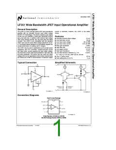
 NSC [ National Semiconductor ]