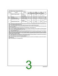
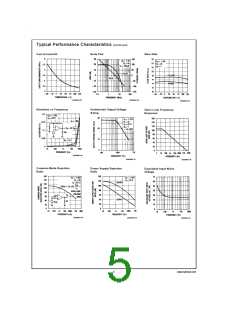
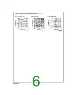
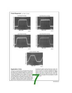
AC Electrical Characteristics (Note 7)
Symbol
Parameter
Conditions
LF147
LF347B
Typ Max Min
LF347
Units
Min
Typ Max Min
−120
Typ Max
−120
=
Amplifier to Amplifier Coupling
TA 25˚C,
−120
dB
=
f
1 Hz−20 kHz
(Input Referred)
=
=
±
SR
Slew Rate
VS 15V, TA 25˚C
8
13
4
8
13
4
8
13
4
V/µs
MHz
=
=
±
GBW
en
Gain-Bandwidth Product
Equivalent Input Noise Voltage
VS 15V, TA 25˚C
2.2
2.2
2.2
=
=
TA 25˚C, RS 100Ω,
20
20
20
=
f
1000 Hz
=
=
in
Equivalent Input Noise Current
Tj 25˚C, f 1000 Hz
0.01
0.01
0.01
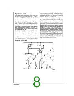
Note 2: Absolute Maximum Ratings indicate limits beyond which damage to the device may occur. Operating Ratings indicate conditions for which the device is func-
tional, but do not guarantee specific performance limits.
Note 3: Unless otherwise specified the absolute maximum negative input voltage is equal to the negative power supply voltage.
Note 4: Any of the amplifier outputs can be shorted to ground indefinitely, however, more than one should not be simultaneously shorted as the maximum junction
temperature will be exceeded.
Note 5: For operating at elevated temperature, these devices must be derated based on a thermal resistance of θ
.
jA
Note 6: The LF147 is available in the military temperature range −55˚C≤T ≤125˚C, while the LF347B and the LF347 are available in the commercial temperature
A
=
range 0˚C≤T ≤70˚C. Junction temperature can rise to T max 150˚C.
A
j
=
=
±
15V for the LF347B/LF347.
±
Note 7: Unless otherwise specified the specifications apply over the full temperature range and for V
20V for the LF147 and for V
S
S
=
are measured at V 0.
CM
V
, I , and I
OS OS
B
Note 8: The input bias currents are junction leakage currents which approximately double for every 10˚C increase in the junction temperature, T . Due to limited pro-
j
duction test time, the input bias currents measured are correlated to junction temperature. In normal operation the junction temperature rises above the ambient tem-
=
perature as a result of internal power dissipation, P . T
D
T
A
+θ
P where θ is the thermal resistance from junction to ambient. Use of a heat sink is recommended
D jA
j
jA
if input bias current is to be kept to a minimum.
Note 9: Supply voltage rejection ratio is measured for both supply magnitudes increasing or decreasing simultaneously in accordance with common practice from
=
=
±
±
±
±
20V to 5V for the LF147.
V
5V to 15V for the LF347 and LF347B and from V
S
S
Note 10: Refer to RETS147X for LF147D and LF147J military specifications.
Note 11: Max. Power Dissipation is defined by the package characteristics. Operating the part near the Max. Power Dissipation may cause the part to operate out-
side guaranteed limits.
Note 12: Human body model, 1.5 kΩ in series with 100 pF.
3
www.national.com

 NSC [ National Semiconductor ]