Electrical Characteristics (Notes 2 and 3) (Continued)
Symbol
Parameter
Conditions
Min
Typ
Max
Units
DS1633/DS3633
e
e
e
e
e
I
I
Supply Currents
V
0V, (Figure 4)
V
CC
V
CC
V
CC
V
CC
5V
Output Low
Output High
7.5
16
2
12
23
4
mA
mA
mA
mA
CC(0)
CC(1)
IN
15V
5V, V
e
(Figure 4)
5V
IN
e
15V, V
IN
15V
7.2
15
e
e
e
e
e
e
e
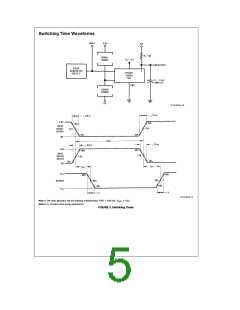
t
t
Propagation to ‘‘1’’
Propagation to ‘‘0’’
V
5V, T
25 C, C
§
15 pF, R
e
15 pF, R
50X, V
10V,
10V,
PD1
PD0
CC
(Figure 5)
A
L
L
L
L
500
750
ns
ns
e
(Figure 5)
e
V
CC
5V, T
25 C, C
§
L
50X, V
A
L
DS1634/DS3634
e
CC
e
I
Supply Currents
(Figure 4)
V
V
V
V
5V, V
IN
5V
Output Low
Output High
7.5
18
3
12
23
5
mA
mA
mA
mA
CC(0)
e
e
e
e
15V
15V, V
5V
CC
CC
CC
IN
e
I
V
V
0V, (Figure 4)
CC(1)
IN
15V
11
18
e
e
e
e
e
e
e
t
t
Propagation to ‘‘1’’
Propagation to ‘‘0’’
5V, T
25 C, C
§
15 pF, R
50X, V
50X, V
10V,
10V,
PD1
PD0
CC
A
L
L
L
L
L
500
750
ns
ns
(Figure 5)
e
(Figure 5)
e
25 C, C
L
e
V
CC
5V, T
15 pF, R
§
A
Note 1: ‘‘Absolute Maximum Ratings’’ are those values beyond which the safety of the device cannot be guaranteed. Except for ‘‘Operating Temperature Range’’
they are not meant to imply that the devices should be operated at these limits. The table of ‘‘Electrical Characteristics’’ provides conditions for actual device
operation.
b
a
Note 2: Unless otherwise specified min/max limits apply across the 55 C to 125 C temperature range for the DS1631, DS1632, DS1633 and DS1634 and
across the 0 C to 70 C range for the DS3631, DS3632, DS3633 and DS3634. All typical values are for T
§
§
a
e
25 C.
§
§
§
A
Note 3: All currents into device pins shown as positive, out of device pins as negative, all voltages referenced to ground unless otherwise noted. All values shown
as max or min on absolute value basis.
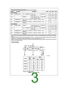
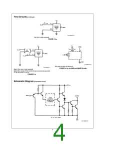
Test Circuits
TL/F/5816–9
Output
Measure
Input
Under
Test
Other
Input
Circuit
Apply
DS3631
DS3632
DS3633
DS3634
V
V
I
V
OH
IH
IH
OH
V
V
CC
I
V
OL
IL
OL
V
IH
V
IH
I
OL
V
OL
V
V
CC
I
V
V
IL
OH
OH
V
IH
GND
I
OH
OH
V
V
I
V
OL
IL
IL
OL
V
IH
GND
I
OL
V
OL
V
IL
V
IL
I
V
OH
OH
Note: Each input is tested separately.
FIGURE 1. V , V , V , V
IH IL OH OL
3

 NSC [ National Semiconductor ]