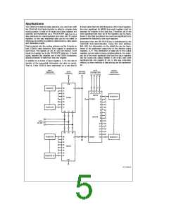
DC Electrical Characteristics CD4514BC, CD4515BC (Note 2) (Continued)
b
a
a
85 C
40 C
§
25 C
§
Typ
§
Symbol
Parameter
Conditions
Units
Min
Max
Min
Max
Min
Max
k
V
IL
Low Level
Input Voltage
I
O
1 mA
5V, V
10V, V
15V, V
l
l
e
e
e
e
0.5V or 4.5V
V
V
V
1.5
3.0
4.0
2.25
4.50
6.75
1.5
3.0
4.0
1.5
3.0
4.0
V
V
V
DD
DD
DD
O
e
1.0V or 9.0V
1.5V or 13.5V
O
e
O
k
1 mA
V
IH
High Level
Input Voltage
I
V
V
V
l
O
l
e
e
0.5V or 4.5V
5V, V
3.5
7.0
11.0
3.5
7.0
11.0
2.75
5.50
8.25
3.5
7.0
11.0
V
V
V
DD
DD
DD
O
e
e
e
1.0V or 9.0V
10V, V
15V, V
O
O
e
1.5V or 13.5V
e
e
e
e
0.4V
I
I
I
Low Level Output
Current (Note 3)
V
V
V
5V, V
O
10V, V
15V, V
0.52
1.3
3.6
0.44
1.1
3.0
0.88
2.25
8.8
0.36
0.90
2.4
mA
mA
mA
OL
OH
IN
DD
DD
DD
e
e
0.5V
1.5V
O
O
e
e
e
e
O
b
b
b
b
High Level Output
Current (Note 3)
V
DD
V
DD
V
DD
5V, V
10V, V
15V, V
4.6V
0.52
0.44
0.88
2.25
8.8
0.36
0.90
mA
mA
mA
e
e
b
b
b
b
b
b
9.5V
13.5V
1.3
3.6
1.1
3.0
O
O
b
b
2.4
b
10b
5
5
e
e
e
e
b
0.3
0.3
b
b
0.3
0.3
b
1.0
1.0
Input Current
V
DD
V
DD
15V, V
15V, V
0V
15V
10
mA
mA
IN
IN
AC Electrical Characteristics*
e
e
e
e
t 20 ns unless otherwise specified
f
All types C
50 pF, T
25 C, t
§
L
A
r
Symbol
Parameter
Transition Times
Conditions
Min
Typ
Max
Units
e
e
e
t
t
t
t
t
, t
THL TLH
V
DD
V
DD
V
DD
5V
10V
15V
100
50
40
200
100
80
ns
ns
ns
e
e
e
, t
PLH PHL
Propagation Delay Times
V
V
V
5V
10V
15V
550
225
150
1100
450
300
ns
ns
ns
DD
DD
DD
e
e
e
, t
PLH PHL
Inhibit Propagation
Delay Times
V
DD
V
DD
V
DD
5V
10V
15V
400
150
100
800
300
200
ns
ns
ns
e
e
e
Setup Time
V
DD
V
DD
V
DD
5V
10V
15V
125
50
38
250
100
75
ns
ns
ns
SU
e
e
e
Strobe Pulse Width
V
DD
V
DD
V
DD
5V
10V
15V
175
50
38
350
100
75
ns
ns
ns
WH
C
C
Power Dissipation Capacitance
Input Capacitance
Per Package (Note 5)
Any Input (Note 4)
150
5
pF
pF
PD
7.5
IN
*AC Parameters are guaranteed by DC correlated testing.
Note 1: ‘‘Absolute Maximum Ratings’’ are those values beyond which the safety of the device cannot be guaranteed. Except for ‘‘Operating Temperature Range’’
they are not meant to imply that the devices should be operated at these limits. The tables of ‘‘Recommended Operating Conditions’’ and ‘‘Electrical Characteris-
tics’’ provide conditions for actual device operation.
e
Note 2: V
0V unless otherwise specified.
and I are tested one output at a time.
SS
Note 3: I
OH
OL
Note 4: Capacitance is guaranteed by periodic testing.
Note 5: C determines the no load AC power consumption of any CMOS device. For complete explanation, see 54C and 74C Family Characteristics application
PD
note, AN-90.
3

 NSC [ National Semiconductor ]