e
e
e
e
t 20 ns, unless otherwise specified
fCL
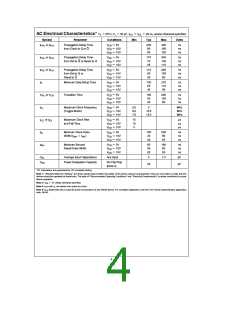
AC Electrical Characteristics* T
25 C, C
§
50 pF, t
rCL
A
L
Symbol
Parameter
Conditions
Min
Typ
Max
Units
e
e
e
t
t
t
t
t
f
t
t
t
or t
or t
or t
Propagation Delay Time
from Clock to Q or Q
V
V
V
5V
200
80
400
160
130
ns
ns
ns
PHL
PHL
PHL
S
PLH
PLH
PLH
DD
DD
DD
10V
15V
65
e
e
e
Propagation Delay Time
V
DD
V
DD
V
DD
5V
170
70
340
140
110
ns
ns
ns
from Set to Q or Reset to Q
10V
15V
55
e
e
e
Propagation Delay Time
from Set to Q or
Reset to Q
V
DD
V
DD
V
DD
5V
110
50
220
100
80
ns
ns
ns
10V
15V
40
e
e
e
Minimum Data Setup Time
V
DD
V
DD
V
DD
5V
135
55
270
110
90
ns
ns
ns
10V
15V
45
e
e
e
or t
Transition Time
V
DD
V
DD
V
DD
5V
100
50
200
100
80
ns
ns
ns
THL
CL
TLH
10V
15V
40
e
e
e
Maximum Clock Frequency
(Toggle Mode)
V
DD
V
DD
V
DD
5V
2.5
6.2
7.6
5
MHz
MHz
MHz
10V
15V
12.5
15.5
e
e
e
or t
fCL
Maximum Clock Rise
and Fall Time
V
DD
V
DD
V
DD
5V
15
10
5
ms
ms
ms
rCL
W
10V
15V
e
e
e
Minimum Clock Pulse
e
V
DD
V
DD
V
DD
5V
100
40
200
80
ns
ns
ns
Width (t
WH
t )
WL
10V
15V
32
65
e
e
e
Minimum Set and
V
DD
V
DD
V
DD
5V
80
30
25
160
60
ns
ns
ns
WH
Reset Pulse Width
10V
15V
50
C
C
Average Input Capacitance
Power Dissipation Capacity
Any Input
5
7.5
pF
pF
IN
Per Flip-Flop
(Note 4)
PD
35
*AC Parameters are guaranteed by DC correlated testing.
Note 1: ‘‘Absolute Maximum Ratings’’ are those values beyond which the safety of the device cannot be guaranteed. They are not meant to imply that the
devices should be operated at these limits. The table of ‘‘Recommended Operating Conditions’’ and ‘‘Electrical Characteristics’’ provides conditions for actual
device operation.
e
Note 2: V
0V unless otherwise specified.
and I are tested one output at a time.
SS
Note 3: I
OH
OL
Note 4: C determines the no load AC power consumption of any CMOS device. For complete explanation, see 54C/74C Family Characteristics application
PD
note, AN-90.
4

 NSC [ National Semiconductor ]