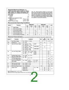
Absolute Maximum Ratings (Note)
If Military/Aerospace specified devices are required,
please contact the National Semiconductor Sales
Office/Distributors for availability and specifications.
Note: The ‘‘Absolute Maximum Ratings’’ are those values
beyond which the safety of the device cannot be guaran-
teed. The device should not be operated at these limits. The
parametric values defined in the ‘‘Electrical Characteristics’’
table are not guaranteed at the absolute maximum ratings.
The ‘‘Recommended Operating Conditions’’ table will define
the conditions for actual device operation.
Supply Voltage
Input Voltage
7V
DIR or G
A or B
7V
5.5V
Operating Free Air Temperature Range
DM54LS and 54LS
DM74LS
b
b
a
55 C to 125 C
§
§
0 C to 70 C
a
§
65 C to 150 C
§
a
Storage Temperature Range
§
§
Recommended Operating Conditions
DM54LS245
DM74LS245
Symbol
Parameter
Units
Min
4.5
2
Nom
Max
Min
4.75
2
Nom
Max
V
V
V
Supply Voltage
5
5.5
5
5.25
V
V
CC
High Level Input Voltage
Low Level Input Voltage
High Level Output Current
Low Level Output Current
Free Air Operating Temperature
IH
0.7
0.8
V
IL
b
b
I
I
12
12
125
15
24
70
mA
mA
OH
OL
b
T
A
55
0
C
§
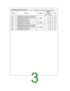
Electrical Characteristics over recommended operating free air temperature range (unless otherwise noted)
Typ
Symbol
Parameter
Conditions
Min
Max
Units
(Note 1)
e
e
e
e b
I
b
1.5
V
Input Clamp Voltage
V
V
Min, I
18 mA
V
V
I
CC
CC
CC
b
HYS
V
Hysteresis (V
V
)
b
Min
0.2
2.7
0.4
a
T
T
e
High Level Output Voltage
V
V
Min, V
Min
DM74
OH
IH
e
e b
Max, I
1 mA
3 mA
IL
OH
e
e
V
V
Min, V
Min
DM54/DM74
DM54/DM74
CC
IL
2.4
2
3.4
V
V
e
e b
Max, I
IL
OH
e
e
e
V
V
Min, V
Min
Max
CC
IH
e
0.5V, I
IL
OH
e
e
e
V
OL
Low Level Output Voltage
V
V
V
Min
Max
Min
I
12 mA
Max
DM74
DM54
DM74
0.4
CC
OL
OL
e
e
IL
I
0.4
0.5
IH
e
e
e
I
I
I
Off-State Output Current,
High Level Voltage Applied
V
V
V
Max
V
V
2.7V
0.4V
OZH
OZL
I
CC
O
20
mA
mA
mA
e
e
Max
IL
Min
IH
Off-State Output Current,
Low Level Voltage Applied
O
b
200
e
e
e
Input Current at Maximum
Input Voltage
V
CC
Max
A or B
DIR or G
V
V
5.5V
7V
0.1
0.1
20
I
I
e
e
e
e
e
I
I
I
I
High Level Input Current
Low Level Input Current
Short Circuit Output Current
Supply Current
V
CC
V
CC
V
CC
Max, V
Max, V
2.7V
0.4V
mA
mA
mA
IH
I
b
0.2
IL
I
b
b
225
Max (Note 2)
40
OS
CC
e
Outputs High
Outputs Low
Outputs at Hi-Z
V
Max
48
62
64
70
90
95
CC
mA
e
e
25 C.
Note 1: All typicals are at V
5V, T
§
Note 2: Not more than one output should be shorted at a time, not to exceed one second duration
CC
A
2

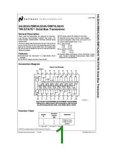
 NSC [ National Semiconductor ]