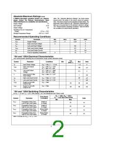
Absolute Maximum Ratings (Note)
If Military/Aerospace specified devices are required,
please contact the National Semiconductor Sales
Office/Distributors for availability and specifications.
Note: The ‘‘Absolute Maximum Ratings’’ are those values
beyond which the safety of the device cannot be guaran-
teed. The device should not be operated at these limits. The
parametric values defined in the ‘‘Electrical Characteristics’’
table are not guaranteed at the absolute maximum ratings.
The ‘‘Recommended Operating Conditions’’ table will define
the conditions for actual device operation.
Supply Voltage
Input Voltage
Output Voltage
7V
5.5V
7V
Operating Free Air Temperature
Range
a
0 C to 70 C
§
§
b
a
65 C to 150 C
Storage Temperature Range
§
§
Recommended Operating Conditions
Symbol
Parameter
Min
4.75
2
Nom
Max
Units
V
V
V
V
V
Supply Voltage
5
5.25
CC
High Level Input Voltage
Low Level Input Voltage
V
IH
0.8
5.5
12
V
IL
High Level Output Voltage
Low Level Output Current
Free Air Operating Temperature
V
OH
I
mA
OL
T
A
0
70
C
§
’184 and ’185A Electrical Characteristics
over recommended operating free air temperature range (unless otherwise noted)
Typ
(Note 1)
Symbol
Parameter
Conditions
e b
Min
Max
Units
e
e
b
1.5
V
I
Input Clamp Voltage
V
Min, I
I
12 mA
V
CC
e
e
I
High Level Output
Current
V
V
Min, V
5.5V
Min
CEX
CC
O
100
0.4
mA
e
Max, V
IL
IH
e
e
V
OL
Low Level Output
Voltage
V
CC
V
IH
Min, I
OL
Min, V
Max
Max
V
e
e
IL
@
Input Current Max
Input Voltage
e
e
I
V
CC
Max, V
5.5V
I
I
1
mA
e
e
e
e
e
I
I
I
High Level Input Current
Low Level Input Current
V
V
V
Max, V
Max, V
Max
2.4V
0.4V
25
mA
IH
CC
CC
CC
I
b
1
mA
IL
I
Supply Current with
Outputs High
CCH
65
80
95
99
mA
mA
e
I
Supply Current with
Outputs Low
V
CC
Max
CCL
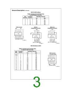
’184 and ’185A Switching Characteristics
5V and T
e
e
25 C (See Section 1 for Test Waveforms and Output Load)
at V
§
CC
A
e
e
600X
15 pF (See Test Circuit)
R
400X, R
L1
L2
From (Input)
To (Output)
e
C
L
Symbol
Parameter
Units
Min
Max
t
t
t
t
Propagation Delay Time
Low to High Level Output
Enable G
to Output
PLH
PHL
PLH
PHL
35
35
35
35
ns
ns
ns
ns
Propagation Delay Time
High to Low Level Output
Enable G
to Output
Propagation Delay Time
Low to High Level Output
Binary Select
to Output
Propagation Delay Time
High to Low Level Output
Binary Select
to Output
e
e
25 C.
Note 1: All typicals are at V
5V, T
§
CC
A
2

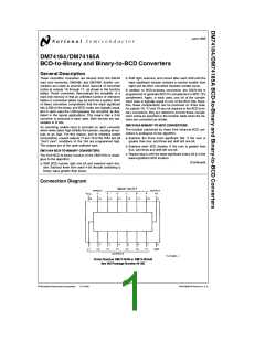
 NSC [ National Semiconductor ]