Integrated Functions (Continued)
4.5.8.1 Configuration and Status Registers
The Configuration and Status Registers group consists of
four 32-bit registers located at GX_BASE+8300h-830Ch.
These registers are described below and Table 4-29 gives
their bit formats.
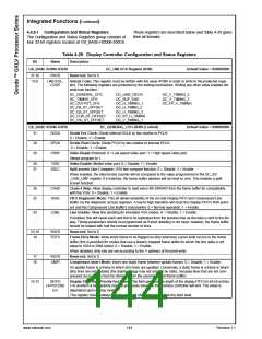
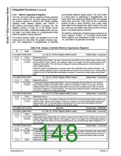
Table 4-29. Display Controller Configuration and Status Registers
Bit
Name
Description
GX_BASE+8300h-8303h
DC_UNLOCK Register (R/W)
Default Value = 00000000h
31:16
15:0
RSVD
Reserved: Set to 0.
UNLOCK_
CODE
Unlock Code: This register must be written with the value 4758h in order to write to the protected regis-
ters. The following registers are protected by the locking mechanism. Writing any other value enables the
write lock function.
DC_GENERAL_CFG
DC_TIMING_CFG
DC_LINE_DELTA
DC_BUF_SIZE
DC_V_TIMING_2
DC_V_TIMING_3
DC_FP_V_TIMING
DC_OUTPUT_CFG
DC_FB_ST_OFFSET
DC_CB_ST_OFFSET
DC_CUR_ST_OFFSET
DC_VID_ST_OFFSET
DC_H_TIMING_1
DC_H_TIMNG_2
DC_H_TIMING_3
DC_FP_H_TIMING
DC_V_TIMING_1
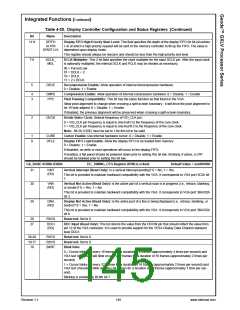
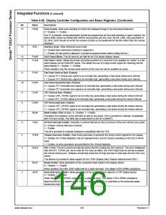
GX_BASE+8304h-8307h
DC_GENERAL_CFG (R/W) (Locked)
Default Value = 00000000h
31
30
29
DDCK
DPCK
VRDY
Divide Dot Clock: Divide internal DCLK by two relative to PCLK:
0 = Disable; 1 = Enable.
Divide Pixel Clock: Divide PCLK by two relative to internal DCLK:
0 = Disable; 1 = Enable.
Video Ready Protocol: 0 = Low speed video port: 1 = High speed video port.
Always program to 1.
28
27
VIDE
Video Enable: Motion video port: 0 = Disable; 1 = Enable.
SSLC
Split-screen Line Compare: VGA line compare function: 0 = Disable; 1 = Enable.
When enabled, the internal line counter will be compared to the value programmed in the DC_SS
_LINE_CMP register. If it matches, the frame buffer address will be reset to zero. This enables a split
screen function.
26
25
CH4S
DIAG
Chain 4 Skip: Allow display controller to read every 4th DWORD from the frame buffer for compatibility
with the VGA: 0 = Disable; 1 = Enable.
FIFO Diagnostic Mode: This bit allows testability of the on-chip Display FIFO and Compressed Line
Buffer via the diagnostic access registers. A low-to-high transition will reset the Display FIFO’s R/W point-
ers and the Compressed Line Buffer’s read pointer. 0 = Normal operation; 1 = Enable.
24
LDBL
Line Double: Allow line doubling for emulated VGA modes: 0 = Disable; 1 = Enable.
If enabled, this will cause each odd line to be replicated from the previous line as the data is sent to the dis-
play. Timing parameters should be programmed as if pixel doubling is not used, however, the frame buffer
should be loaded with half the normal number of lines.
23:19
18
RSVD
FDTY
Reserved: Set to 0.
Frame Dirty Mode: Allow entire frame to be flagged as dirty whenever a pixel write occurs to the frame
buffer (this is provided for modes that use a linearly mapped frame buffer for which the line delta is not
equal to 1024 or 2048 bytes): 0 = Disable; 1 = Enable.
When disabled, dirty bits are set according to the Y address of the pixel write.
Reserved: Set to 0.
17
16
RSVD
CMPI
Compressor Insert Mode: Insert one static frame between update frames: 0 = Disable; 1 = Enable.
An update frame is a frame in which dirty lines are updated. Conversely, a static frame is a frame in which
dirty lines are not updated (the display image may not actually be static, because lines that are not com-
pressed successfully must be retrieved from the uncompressed frame buffer).
15:12
DFIFO
Display FIFO High Priority End Level: This field specifies the depth of the display FIFO (in 64-bit entries
HI-PRI END x 4) at which a high-priority request previously issued to the memory controller will end. The value is
LVL
dependent upon display mode.
This register should always be non-zero and should be larger than the start level.
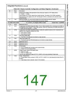
www.national.com
144
Revision 1.1

 NSC [ National Semiconductor ]