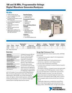
100 and 50 MHz, Programmable-Voltage
Digital Waveform Generator/Analyzers
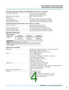
Specifications
These specifications are valid for the following temperature ranges: PXI: 0 to 55 °C, PCI: 0 to 45 °C.
Channel Characteristics
Number of data channels ...................................................... 20
Direction control of data channels........................................ Per-channel, per-cycle
Generation Signal Characteristics (data, DDC ClkOut, and PFI <0..3> channels)
All voltage ranges specified into 1 M
Ω
Generation voltage range...................................................... -2.0 to 5.5 V
Generation signal type .......................................................... Single-ended
Number of programmable voltage levels.............................. 1 voltage low level and 1 voltage high level applies to all data,
Clk Out (sample clock only), and PFI channels
Generation voltage range restrictions................................... -0.5 to 5.5 V (up to 50 MHz clock rate)
-2 to 3.7 V (up to 50 MHz clock rate)
-0.5 to 3.7 V (50 to 100 MHz clock rate; NI 6552 only)
Generation voltage swing ..................................................... 400 mV to 6 V (up to 50 MHz clock rate)
400 mV to 4.2 V (50 to 100 MHz clock rate; NI 6552 only)
Generation voltage-level resolution...................................... 10 mV
DC generation voltage-level accuracy................................... 20 mV (excluding system crosstalk)
Output impedance.................................................................. 50
Maximum DC drive strength.................................................. 50 mA maximum per channel
600 mA maximum for all data, clock, and PFI channels
Channel power-up state ........................................................ Drivers disabled, 10 k input impedance
Ωnominal at 25 °C
Ω
Acquisition Signal Characteristics (data, strobe, and PFI <0..3> channels)
Acquisition voltage range...................................................... -2.0 V to 5.5 V
Number of programmable acquisition thresholds ................ 1 voltage low threshold and a strobe voltage high threshold applies to all data
and PFI channels
Minimum detectable voltage swing...................................... 50 mV
Acquisition voltage threshold resolution .............................. 10 mV
DC acquisition voltage threshold accuracy........................... 30 mV (excluding system crosstalk)
Input impedance .................................................................... 50
Ω
or 10 kΩ(default), software-selectable per channel;
applies when powered on and within valid voltage range
Timing Characteristics
Sample Clock
Sample clock sources ............................................................ 1. Onboard clock (internal VCXO with divider)
2. CLK IN (SMB jack connector)
3. PXI_STAR (PXI backplane; PXI only)
4. STROBE (DDC Connector) – Acquisition only
Onboard clock frequency range ............................................ NI 6551: 48 Hz to 50 MHz. (settable to 200 MHz/N; 4
NI 6552: 48 Hz to 100 MHz (settable to 200 MHz/N; 2
≤
N
≤
4,194,304)
≤N ≤4,194,304)
Exported sample clock delay range....................................... 0 to 1 sample clock periods for clock frequencies
≥25 MHz
Exported sample clock delay resolution................................ 1/256 of sample clock period for clock frequencies
≥25 MHz
Exported Sample Clock Jitter (typical using onboard clock)
Period jitter
Cycle-to-cycle jitter
20 ps (rms)
35 ps (rms)
BUY ONLINE at ni.com or CALL (866) 265 9891 (U.S.)
3

 NI [ National Instruments ]