µPD75216A
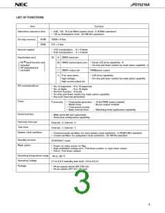
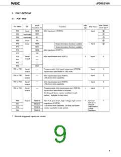
LIST OF FUNCTIONS
Item
Function
Instruction execution time
• 0.95, 1.91, 15.3 µs (Main system clock : 4.19 MHz operation)
• 122 µs (Subsystem clock : 32.768 kHz operation)
On-chip memory
General register
ROM
RAM
16256 × 8 bits
512 × 4 bits
• 4-bit manipulation : 8 × 4 banks
• 8-bit manipulation : 4 × 4 banks
Input/output port
®
33
8
CMOS input pin
FIP dual-function pin
included
20 CMOS input/output pins • Direct LED drive capability : 8
On-chip pull-down resistor by mask option capability : 4
•
FIP dedicated pin
excluded
1
4
CMOS output pin
PWM/pulse output
P-ch open-drain,
high-voltage,
• LED drive capability
•
On-chip pull-down resistor by mask option capability
high-current output pin
FIP controller/driver
• No. of segments : 9 to 16 segments
• No. of digits : 9 to 16 digits
• Dimmer function : 8 levels
• On-chip pull-down resistor by mask option capability
• Key scan interrupt generation
Timer
4 channels
• Timer/pulse generator : 14-bit PWM output enabled
• Watch timer
: Buzzer output enabled
• Timer/event counter
• Basic interval timer
: Watchdog timer application capability
Serial interface
• MSB start/LSB start switchable
• Serial bus configuration capability
Vectored interrupt
Test input
External : 3, Internal : 5
External : 1, Internal : 1
System clock oscillator
• Ceramic/crystal oscillator for main system clock oscillation : 4.194304 MHz standard
• Crystal oscillator for subsystem clock oscillation : 32.768 kHz standard
Standby function
Mask option
STOP/HALT mode
• Power-on reset, power-on flag
• High withstand voltage port : Pull-down resistor or open-drain output
• Port 6 : Pull-down resistor
Operating temperature range
Operating voltage
Package
–40 to +85 °C
2.7 to 6.0 V (standby data hold : 2.0 to 6.0 V)
• 64-pin plastic shrink DIP (750 mil)
• 64-pin plastic QFP (14 × 20 mm)
3

 NEC [ NEC ]