CHAPTER 1 INTRODUCTION
(2/2)
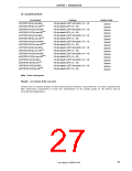
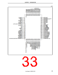
Notes 1. IC pin:
Connect directly to VSS (µPD703212, 703212Y, 703213, 703213Y, 703214, 703214Y,
703215, 703215Y).
VPP pin:
Connect to VSS in normal operation mode (µPD70F3214, 70F3214Y).
FLMD0 pin: Connect to VSS in normal operation mode (µPD70F3214H, 70F3214HY, 70F3215H,
70F3215HY).
FLMD1 pin: Used only in the µPD70F3214H, 70F3214HY, 70F3215H, and 70F3215HY.
2. When using a regulator, connect the REGC pin to VSS via a 10 µF capacitor.
When not using a regulator, connect the REGC pin directly to VDD.
3. The TIP00, TOP00, TIP01, and TOP01 pins can be used only in the µPD703215, 703215Y,
70F3215H, and 70F3215HY.
4. The SCL0 and SDA0 pins can be used only in the µPD703212Y, 703213Y, 703214Y, 703215Y,
70F3214Y, 70F3214HY, and 70F3215HY.
Caution Make EVDD the same potential as VDD.
BVDD can be used when VDD = EVDD ≥ BVDD.
31
User’s Manual U16890EJ1V0UD

 NEC [ NEC ]