CHAPTER 4 PORT FUNCTIONS
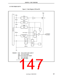
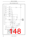
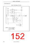
Figure 4-2. Block Diagram of P02 to P06
EVDD
WRPU
WRINTR
WRINTF
WRPMC
WRPM
PU0
P-ch
PU0n
INTR0
INTR0n
INTF0
INTF0n
PMC0
PMC0n
PM0
PM0n
WRPORT
P02/NMI,
P03/INTP0,
P04/INTP1,
P05/INTP2,
P06/INTP3
Output latch
(P0n)
Address
RD
NMI, INTP0 to INTP3 input
Noise eliminator
Edge detector
Remarks 1. PU0: Pull-up resistor option register 0
PM0: Port 0 mode register
PMC0: Port 0 mode control register
INTF0: External interrupt falling edge specification register 0
INTR0: External interrupt rising edge specification register 0
RD: Port 0 read signal
WR: Port 0 write signal
2. n = 2 to 6
User’s Manual U15862EJ3V0UD
148

 NEC [ NEC ]