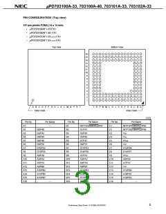
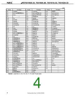
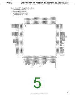
µPD703100A-33, 703100A-40, 703101A-33, 703102A-33
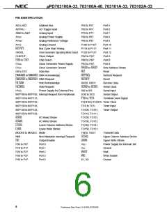
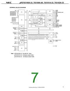
PIN IDENTIFICATION
A0 to A23:
ADTRG:
ANI0 to ANI7:
AVDD:
Address Bus
P50 to P57:
P60 to P67:
P70 to P77:
P80 to P87:
P90 to P97:
P100 to P107:
P110 to P117:
Port 5
AD Trigger Input
Port 6
Analog Input
Port 7
Analog Power Supply
Analog Reference Voltage
Analog Ground
Port 8
AVREF:
Port 9
AVSS:
Port 10
BCYST:
CKSEL:
CLKOUT:
CS0 to CS7:
CVDD:
Bus Cycle Start Timing
Port 11
Clock Generator Operating Mode Select P120 to P127:
Port 12
Clock Output
PA0 to PA7:
PB0 to PB7:
PX5 to PX7:
RAS0 to RAS7:
RD:
Port A
Chip Select
Port B
Clock Generator Power Supply
Clock Generator Ground
Data Bus
Port X
CVSS:
Row Address Strobe
Read
D0 to D15:
DMAAK0 to DMAAK3: DMA Acknowledge
DMARQ0 to DMARQ3: DMA Request
REFRQ:
Refresh Request
Reset
RESET:
HLDAK:
HLDRQ:
HVDD:
Hold Acknowledge
RXD0, RXD1:
SCK0 to SCK3:
SI0 to SI3:
SO0 to SO3:
TC0 to TC3:
Receive Data
Serial Clock
Serial Input
Serial Output
Terminal Count Signal
Hold Request
Power Supply for External Pins
INTP100 to INTP103, Interrupt Request from Peripherals
INTP110 to INTP113,
INTP120 to INTP123,
TCLR10 to TCLR15: Timer Clear
INTP130 to INTP133,
TI10 to TI15:
TO100, TO101,
TO110, TO111,
TO120, TO121,
TO130, TO131,
TO140, TO141,
TO150, TO151:
TXD0, TXD1:
UCAS:
Timer Input
INTP140 to INTP143,
Timer Output
INTP150 to INTP153
:
IORD:
I/O Read Strobe
IOWR:
I/O Write Strobe
LCAS:
Lower Column Address Strobe
Lower Write Strobe
LWR:
MODE0 to MODE3: Mode
Transmit Data
NMI:
Non-Maskable Interrupt Request
Upper Column Address Strobe
Upper Write Strobe
Power Supply for Internal Unit
Ground
OE:
Output Enable
Port 0
UWR:
P00 to P07:
P10 to P17:
P20 to P27:
P30 to P37:
P40 to P47:
VDD:
Port 1
VSS:
Port 2
WAIT:
Wait
Port 3
WE:
Write Enable
Port 4
X1, X2:
Crystal
6
Preliminary Data Sheet U14168EJ2V0DS00

 NEC [ NEC ]