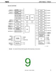
µPD178023, 178024
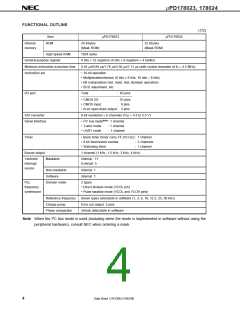
FUNCTIONAL OUTLINE
(1/2)
Item
µPD178023
µPD178024
Internal
memory
ROM
24 Kbytes
32 Kbytes
(Mask ROM)
(Mask ROM)
High-speed RAM
1024 bytes
General-purpose register
Minimum instruction execution time
Instruction set
8 bits × 32 registers (8 bits × 8 registers × 4 banks)
0.45 µs/0.89 µs/1.78 µs/3.56 µs/7.11 µs (with crystal resonator of fX = 4.5 MHz)
• 16-bit operation
• Multiplication/division (8 bits × 8 bits, 16 bits ÷ 8 bits)
• Bit manipulation (set, reset, test, Boolean operation)
• BCD adjustment, etc.
I/O port
Total
: 62 pins
• CMOS I/O
: 53 pins
• CMOS input
: 6 pins
• N-ch open-drain output : 3 pins
A/D converter
Serial interface
8-bit resolution × 6 channels (VDD = 4.5 to 5.5 V)
• I2C bus modeNote: 1 channel
• 3-wire mode
• UART mode
: 1 channel
: 1 channel
Timer
• Basic timer (timer carry FF (10 Hz)) : 1 channel
• 8-bit timer/event counter
• Watchdog timer
: 2 channels
: 1 channel
Buzzer output
1 channel (1 kHz, 1.5 kHz, 3 kHz, 4 kHz)
Vectored
interrupt
source
Maskable
Internal : 11
External: 5
Non-maskable
Software
Internal: 1
Internal: 1
PLL
Division mode
2 types
frequency
synthesizer
• Direct division mode (VCOL pin)
• Pulse swallow mode (VCOL and VCOH pins)
Reference frequency
Charge pump
Seven types selectable in software (1, 3, 9, 10, 12.5, 25, 50 kHz)
Error out output: 2 pins
Phase comparator
Unlock detectable in software
Note When the I2C bus mode is used (including when the mode is implemented in software without using the
peripheral hardware), consult NEC when ordering a mask.
4
Data Sheet U14126EJ1V0DS00

 NEC [ NEC ]