CHAPTER 2 PIN FUNCTIONS
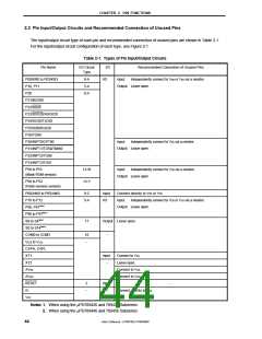
2.3 Pin Input/Output Circuits and Recommended Connection of Unused Pins
The input/output circuit type of each pin and recommended connection of unused pins are shown in Table 2-1.
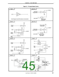
For the input/output circuit configuration of each type, see Figure 2-1.
Table 2-1. Types of Pin Input/Output Circuits
Pin Name
I/O Circuit
Type
I/O
Recommended Connection of Unused Pins
P00/KR0 to P03/KR3
P10, P11
8-A
5-A
8-A
I/O
Input:
Independently connect to VDD or VSS via a resistor.
Output: Leave open.
P20
P21/BZO90
P22/SS20
P23/SCK20/ASCK20
P24/SO20/TxD20
P25/SI20/RxD20
P26/TO90
P30/INPT0/CPT90
P31/INPT1/TO50/TMI60
P32/INPT2/TO60
P33/INPT3/TO61
Input:
Independently connect to VSS via a resistor.
Output: Leave open.
P50 to P53
13-W
13-V
Input:
Independently connect to VDD via a resistor.
(Mask ROM version)
Output: Leave open.
P50 to P53
(Flash memory version)
P60/ANI0 to P65/ANI5
P70 to P72
P80, P81Note 1
P90 to P97Note 1
S0 to S4Note 1
S0 to S14Note 2
COM0 to COM3
VLC0 to VLC2
CAPH, CAPL
XT1
9-C
5-A
Input
I/O
Connect directly to VDD or VSS.
Input:
Independently connect to VDD or VSS via a resistor.
Output: Leave open.
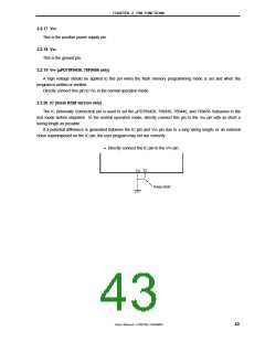
17
Output Leave open.
18
•−•
−
Input
Connect to VSS.
Leave open.
XT2
−
AVSS
Connect to VSS.
Connect to VDD.
AVDD
RESET
2
Input
−
IC
−
•−•
Connect directly to VSS.
VPP
Notes 1. When using the µPD789426 and 789436 Subseries
2. When using the µPD789446 and 789456 Subseries
44
User’s Manual U15075EJ1V0UM00

 NEC [ NEC ]