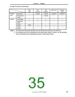
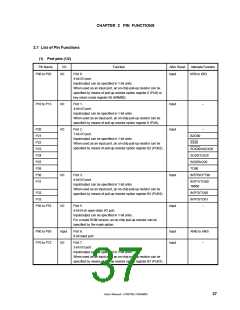
CHAPTER 2 PIN FUNCTIONS
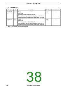
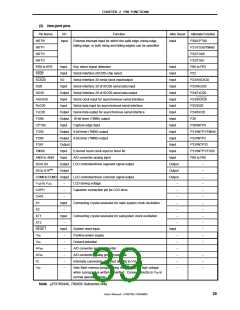
(2) Non-port pins
Pin Name
INTP0
I/O
Function
After Reset
Input
Alternate Function
Input
P30/CPT90
External interrupt input for which the valid edge (rising edge,
falling edge, or both rising and falling edges) can be specified
INTP1
P31/TO50/TMI60
INTP2
P32/TO60
INTP3
P33/TO61
KR0 to KR3
SS20
Input
Input
I/O
Key return signal detection
Input
Input
Input
Input
Input
Input
Input
Input
Input
Input
Input
Input
Input
Input
Input
Output
Output
Output
−
P00 to P03
Serial interface (SIO20) chip select
Serial interface 20 serial clock input/output
Serial interface 20 of SIO20 serial data input
P22
SCK20
SI20
P23/ASCK20
Input
P25/RxD20
SO20
Output Serial interface 20 of SIO20 serial data output
P24/TxD20
ASCK20
RxD20
TxD20
Input
Input
Serial clock input for asynchronous serial interface
Serial data input for asynchronous serial interface
P23/SCK20
P25/SI20
Output Serial data output for asynchronous serial interface
Output 16-bit timer (TM90) output
P24/SO20
TO90
P26
CPT90
TO50
Input
Capture edge input
P30/INTP0
Output 8-bit timer (TM50) output
Output 8-bit timer (TM60) output
Output
P31/INTP1/TMI40
TO60
P32/INTP2
TO61
P33/INTP33
TMI60
Input
Input
External count clock input to timer 40
A/D converter analog input
P31/INTP1/TO50
ANI0 to ANI5
S0 to S4
S5 to S14Note
P60 to P65
Output LCD controller/driver segment signal output
Output
•−•
•−•
−
COM0 to COM3 Output LCD controller/driver common signal output
VLC0 to VLC2
CAPH
CAPL
X1
−
LCD driving voltage
•−•
•−•
•−•
•−•
•−•
•−•
•−•
•−•
•−•
•−•
−
Capacitor connection pin for LCD drive
−
−
−
Input
Connecting crystal resonator for main system clock oscillation
Connecting crystal resonator for subsystem clock oscillation
−
X2
−
−
XT1
Input
−
XT2
−
−
RESET
VDD
Input
System reset input
Input
−
−
−
−
−
−
−
Positive power supply
VSS
Ground potential
−
AVDD
AVSS
IC
A/D converter analog potential
A/D converter analog ground potential
Internally connected. Connect directly to VSS.
−
−
•−•
•−•
•−•
−
VPP
Sets flash memory programming mode. Applies high voltage
when a program is written or verified. Connect directly to VSS in
normal operation mode.
−
Note µPD789446, 789456 Subseries only
User’s Manual U15075EJ1V0UM00
39

 NEC [ NEC ]