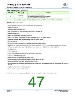
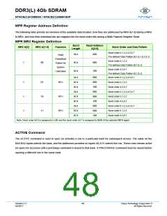
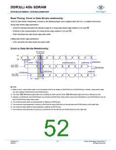
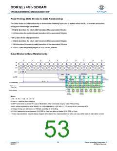
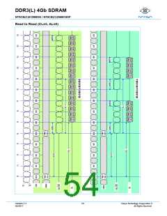
DDR3(L) 4Gb SDRAM
NT5CB(C)512M8DN / NT5CB(C)256M16DP
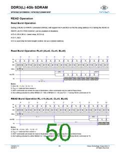
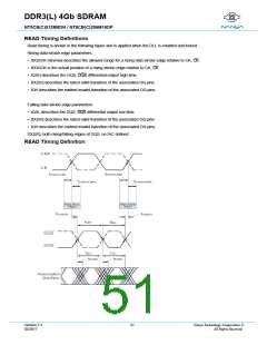
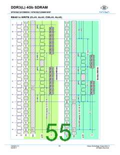
READ Timing Definitions
Read timing is shown in the following figure and is applied when the DLL is enabled and locked.
Rising data strobe edge parameters:
• tDQSCK min/max describes the allowed range for a rising data strobe edge relative to CK, .
• tDQSCK is the actual position of a rising strobe edge relative to CK, .
• tQSH describes the DQS, differential output high time.
• tDQSQ describes the latest valid transition of the associated DQ pins.
• tQH describes the earliest invalid transition of the associated DQ pins.
Falling data strobe edge parameters:
• tQSL describes the DQS, differential output low time.
• tDQSQ describes the latest valid transition of the associated DQ pins.
• tQH describes the earliest invalid transition of the associated DQ pins.
tDQSQ; both rising/falling edges of DQS, no tAC defined.
READ Timing Definition
Version 2.3
02/2017
51
Nanya Technology Cooperation ©
All Rights Reserved.

 NANYA [ Nanya Technology Corporation. ]