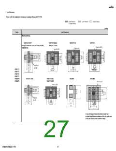
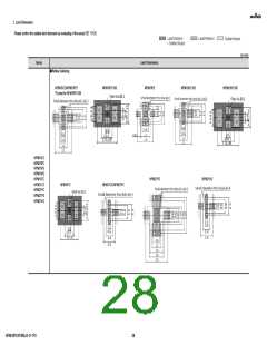
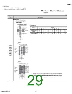
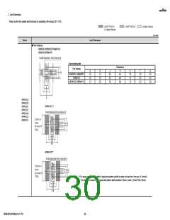
2. Land Dimensions
Please confirm the suitable land dimension by evaluating of the actual SET / PCB.
(in mm)
Series
Land Dimensions
●Reflow Soldering
NFM3DCC/NFM3DPC/NFM31PC/
NFM41CC/NFM41PC
Chip mounting side
Part Number
Dimensions
a
b
c
d
e
f
g
2.4
3.0
3.0
NFM3DCC/ NFM3DPC
NFM31PC
NFM41CC/ NFM41PC
1.0
1.0
1.5
1.4
1.4
2.0
2.5
2.5
3.5
4.4
4.4
6.0
1.0
1.2
1.2
2.0
2.6
2.6
NFM31KC *1
NFM3DCC
NFM3DPC
NFM31PC
NFM31KC
NFM31HK
NFM41CC
NFM41PC
NFM31HC*1
*1 For large current design, width of signal land pattern should be wider not less than 1mm per 1A (1mm/A).
For example, in case of 10A, signal land pattern width should be 10mm or more. (1mm/A*10A=10mm)
NFM18PC474R0J3-0-770
29

 MURATA [ muRata ]