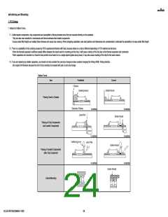
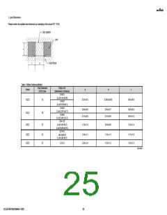
2. Land Dimensions
Please confirm the suitable land dimension by evaluating of the actual SET / PCB.
Table 1 Reflow Soldering Method
Chip Dimension
(L/W) Code
Chip(L×W)
(Dimensions Tolerance)
1.0×0.5
Series
a
b
c
(L:±0.1,W:±0.05)
1.0×0.5
GC□
15
0.3 to 0.5
0.35 to 0.45
0.4 to 0.6
(L:±0.15,W:±0.1)
1.6×0.8
(L:±0.2,W:±0.1)
1.6×0.8
(L:±0.3,W:±0.2)
2.0×1.25
0.6 to 0.8
0.7 to 0.9
0.6 to 0.7
0.7 to 0.8
0.6 to 0.8
0.8 to 1.0
GC□
GC□
18
21
(L:±0.3,W:±0.2)
(L:±0.35,W:±0.25)
3.2×1.6
1.2 to 1.4
0.6 to 0.8
1.2 to 1.4
GC□
GC□
31
32
(±0.3)(±0.4)
(L:±0.4,W:±0.3)
1.9 to 2.1
2.0 to 2.4
1.0 to 1.3
1.0 to 1.2
1.7 to 1.9
1.8 to 2.3
3.2×2.5
(in mm)
GCJ216R72A222MA01-02D
25

 MURATA [ muRata ]