Notice
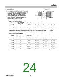
2. Land Dimensions
Chip Capacitor
2-1. Chip capacitors can be cracked due to the stress
of PCB bending , etc. if the land area is larger than
needed and has an excess amount of solder.
Please refer to the land dimensions in table 1
for flow soldering, table 2 for reflow soldering.
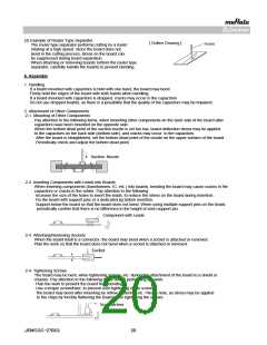
Land
Please confirm the suitable land dimension by
evaluating of the actual SET / PCB.
b
a
Solder Resist
Table 1 Flow Soldering Method
ChipꢀDimension
(L/W)ꢀCode
Series
GC□
GC□
GC□
Chip(L×W)
a
b
c
18
1.6×0.8
2.0×1.25
3.2×1.6
0.6 to 1.0
1.0 to 1.2
2.2 to 2.6
0.8 to 0.9
0.9 to 1.0
1.0 to 1.1
0.6 to 0.8
0.8 to 1.1
1.0 to 1.4
21
31
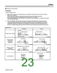
Flow soldering can only be used for products with a chip size of 1.6x0.8mm to 3.2x1.6mm.
(in mm)
Table 2 Reflow Soldering Method
ChipꢀDimension
(L/W)ꢀCode
Series
Chip(L×W)
a
b
c
GC□
GC□
GC□
GC□
GC□
GC□
03
15
18
21
31
32
0.6×0.3
1.0×0.5
1.6×0.8
2.0×1.25
3.2×1.6
3.2×2.5
0.2 to 0.3
0.3 to 0.5
0.6 to 0.8
1.0 to 1.2
2.2 to 2.4
2.0 to 2.4
0.2 to 0.35
0.35 to 0.45
0.6 to 0.7
0.6 to 0.7
0.8 to 0.9
1.0 to 1.2
0.2 to 0.4
0.4 to 0.6
0.6 to 0.8
0.8 to 1.1
1.0 to 1.4
1.8 to 2.3
(in mm)
JEMCGC-2702Q
24

 MURATA [ muRata ]