Notice
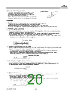
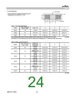
2. Land Dimensions
Chip Capacitor
ꢀPlease confirm the suitable land dimension by
Land
evaluating of the actual SET / PCB.
b
a
Solder Resist
Table 1 Flow Soldering Method
ChipꢀDimension
(L/W)ꢀCode
Series
Chip(L×W)
1.6×0.8
a
b
c
GC□
GC□
GC□
18
21
31
0.6 to 1.0
1.0 to 1.2
2.2 to 2.6
0.8 to 0.9
0.9 to 1.0
1.0 to 1.1
0.6 to 0.8
0.8 to 1.1
1.0 to 1.4
2.0×1.25
3.2×1.6
Flow soldering can only be used for products with a chip size of 1.6x0.8mm to 3.2x1.6mm.
(in mm)
Resistance to PCB bending stress may be improved by designing the “a” dimension with solder resist.
Table 2 Reflow Soldering Method
Chip(L×W)
ChipꢀDimension
(L/W)ꢀCode
Series
(Dimensions
Tolerance)
0.6×0.3
a
b
c
GC□
03
0.2 to 0.25
0.3 to 0.5
0.4 to 0.6
0.6 to 0.8
0.7 to 0.9
1.2
0.2 to 0.3
0.35 to 0.45
0.4 to 0.5
0.6 to 0.7
0.7 to 0.8
0.6 to 0.8
0.25 to 0.35
0.4 to 0.6
0.5 to 0.7
0.6 to 0.8
0.8 to 1.0
1.2 to 1.4
(±0.03)
1.0×0.5
(within ±0.10)
1.0×0.5
GC□
GC□
15
18
(±0.20)
1.6×0.8
(±0.10)
1.6×0.8
(±0.20)
2.0×1.25
(±0.15)
2.0×1.25
(±0.20)
3.2×1.6
(within±0.20)
3.2×1.6
GC□
21
1.0 to 1.4
1.8 to 2.0
1.9 to 2.1
2.0 to 2.4
0.6 to 0.8
0.9 to 1.2
1.0 to 1.3
1.0 to 1.2
1.2 to 1.4
1.5 to 1.7
1.7 to 1.9
1.8 to 2.3
GC□
GC□
31
32
(±0.30)
3.2×2.5
(in mm)
JEMCGC-2702S
24

 MURATA [ muRata ]