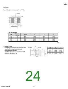
2. Land Dimensions
Please confirm the suitable land dimension by evaluating of the actual SET / PCB.
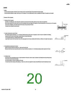
Table 1 Reflow Soldering Method
Chip Dimension
Series
Chip(L×W)
a
b
c
(L/W) Code
GA□
GA□
GA□
GA□
42
43
52
55
4.5×2.0
4.5×3.2
5.7×2.8
5.7×5.0
2.8 to 3.4
3.0 to 3.5
4.0 to 4.6
4.0 to 4.6
1.2 to 1.4
1.2 to 1.4
1.4 to 1.6
1.4 to 1.6
1.4 to 1.8
2.3 to 3.0
2.1 to 2.6
3.5 to 4.8
(in mm)
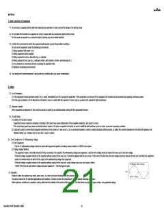
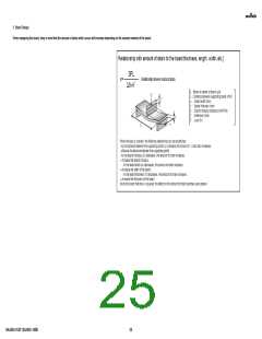
2-2. Dimensions of Slit (Example)
L×W
d
e
Preparing the slit helps flux cleaning and resin coating on the back of the capacitor.
However, the length of the slit design should be as short as possible
to prevent mechanical damage in the capacitor.
A longer slit design might receive more severe mechanical stress from the PCB.
Recommended slit design is shown in the Table.
4.5×2.0
4.5×3.2
5.7×2.8
5.7×5.0
1.0 to 2.8
1.0 to 2.8
1.0 to 4.0
1.0 to 4.0
3.6 to 4.1
4.8 to 5.3
4.4 to 4.9
6.6 to 7.1
GA342A1XGF120JW31-B0B
24

 MURATA [ muRata ]