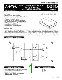
ABSOLUTE MAXIMUM RATINGS
VINP
TST
TLD
Storage Temperature Range . . -65°C to +150°C
Lead Temperature . . . . . . . . . . . . . . . . . 3 0 0 ° C
(10 Seconds Soldering)
Operating Temperature
MSK 5215 Series. . . . . . . . . . -40°C to +85°C
MSK 5215H/E Series . . . . . . . . -55°C to +125°C
Input Voltage (100mS 1%D.C.)-20V to +60V
VIN
VEN
IOUT
Input Voltage
Enable Voltage
Output Current
26V
-0.3V to 26V
3.5A
TJ
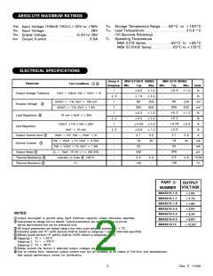
ELECTRICAL SPECIFICATIONS
MSK 5215 SERIES
Group A
MSK 5215H/E SERIES
Parameter
Test Conditions
1
3
Min.
Typ.
Max.
Subgroup Min.
Typ.
Max.
1.0
2.0
200
600
1.0
2.0
0.5
1.0
3.5
30
Units
%
0.5
0.5
1
-
-
-
-
-
-
-
-
-
-
-
-
-
-
-
-
-
-
-
-
-
-
-
-
-
-
-
-
1.0
-
Output Voltage Tolerance
IOUT = 10mA; VIN = VOUT +1V
-
1.0
80
2, 3
%
80
225
625
1.2
-
∆VOUT = -1%; IOUT = 100 mA
∆VOUT = -1%; IOUT = 1.5A
1
mV
mV
%
Dropout Voltage
Load Regulation 8
Line Regulation
2
350
0.2
0.3
0.05
0.5
2.1
18
350
0.2
0.3
0.05
0.5
2.1
18
1
1
10 mA ≤ IOUT ≤ 1.25A
2, 3
%
(VOUT +1V) ≤ VIN ≤ 26V
IOUT = 10 mA
1
0.6
-
%
2, 3
%
3.5
30
-
Output Current Limit 2
VOUT = 0V; VIN = VOUT +1V
VIN = VOUT +1V; IOUT = 0.75A
VIN = VOUT +1V; IOUT = 1.5A
CL = 10µF; 10 HZ ≤ f ≤ 100 KHZ
Junction to Case @ 125°C
TJ
-
-
-
-
-
-
A
mA
mA
µV
°C/W
°C
Ground Current
2
32
32
-
400
3.5
130
400
3.5
130
-
Output Noise 2
-
Thermal Resistance 2
Thermal Shutdown 2
4.0
-
4.5
-
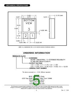
PART 7
NUMBER
OUTPUT
VOLTAGE
MSK5215-1.5
MSK5215-1.7
MSK5215-1.9
MSK5215-2.5
MSK5215-3.3
MSK5215-5.0
MSK5215-12
+1.5V
+1.7V
+1.9V
+2.5V
+3.3V
+5.0V
+12.0V
NOTES:
1 Output decoupled to ground using 33µF minimum capacitor unless otherwise specified.
2 Guaranteed by design but no tested. Typical parameters are representative of actual
device performance but are for reference only.
3 All output parameters are tested using a low duty cycle pulse to maintain TJ = TC.
4 Industrial grade and "E" suffix devices shall be tested to subgroup 1 unless otherwise specified.
5 Military grade devices ('H' suffix) shall be 100% tested to subgroups 1,2,3.
TC = +25°C
TJ = +125°C
TA = -55°C
6 Subgroup 1
Subgroup 2
Subgroup 3
7 Please consult the factory if alternate output voltages are required.
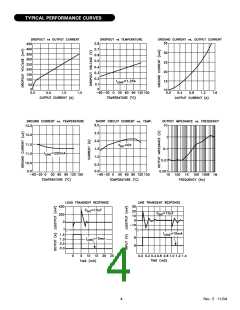
8 Due to current limit, maximum output current may not be available at all values of VIN-VOUT and temperatures.
See typical performance curves for clarification.
2
Rev. E 11/04

 MSK [ M.S. KENNEDY CORPORATION ]